

In the world of GPUs, 2022 will go down as a milestone in their history. Intel made good on its promise of re-entering the discrete graphics card market, Nvidia pushed card sizes and prices through the roof, and AMD brought CPU tech into the graphics arena. The news headlines ran replete with stories of disappointing performance, melting cables, and faked frames.
GPU fervor spilled into forums, with PC enthusiasts amazed and aghast in equal measure, as to what had become of the graphics card market. So, it’s easy to forget that the latest products are housing the most complex and powerful chips that have ever graced a home computer.
Let’s bring all the vendors to the table, and dive deep into their architectures, peeling away the layers to see what’s new, what they have in common, and just what any of this means to the average user. This is a long article, with many sections, so use the following index to navigate through it. You may also want to brush up on RDNA 2 and Ampere architectures before you start here.
Article Index
Overall GPU Structure: Starting From the Top
Let’s start with an important aspect of this article — this is not a performance comparison. Instead, we’re looking at how everything is arranged inside a GPU, checking out the stats and figures to understand the differences in approach that AMD, Intel, and Nvidia have when it comes to designing their graphics processors.
We’ll begin with a look at the overall GPU compositions for the largest chips available that use the architectures we’re examining. It’s important to stress that Intel’s offering isn’t targeted at the same market as AMD’s or Nvidia’s, as it’s very much a mid-range graphics processor.
All three are quite different in size, not only to each other, but also to similar chips using previous architectures. All of this analysis is purely for understanding what exactly is under the hood in all three processors. We’ll examine the overall structures, before breaking apart the fundamental sections of each GPU — the shader cores, ray tracing abilities, the memory hierarchy, and the display and media engines.
AMD Navi 31
Taking things alphabetically, the first on the table is AMD’s Navi 31, their largest RDNA 3-powered chip announced so far. Compared to the Navi 21, we can see a clear growth in component count from their previous top-end GPU…

The Shader Engines (SE) house fewer Compute Units (CUs), 16 versus 200, but there are now 6 SEs in total — two more than before. This means Navi 31 has up to 96 CUs, fielding a total of 6144 Stream Processors (SP). AMD has done a full upgrade of the SPs for RDNA 3 and we’ll tackle that later in the article.
Each Shader Engine also contains a dedicated unit to handle rasterization, a primitive engine for triangle setup, 32 render output units (ROPs), and two 256kB L1 caches. The last aspect is now double the size but the ROP count per SE is still the same.
AMD hasn’t changed the rasterizer and primitive engines much either — the stated improvements of 50% are for the full die, as it has 50% more SEs than the Navi 21 chip. However, there are changes to how the SEs handle instructions, such as faster processing of multiple draw commands and better management of pipeline stages, which should reduce how long a CU needs to wait before it can move on to another task.
The most obvious change is the one that garnered the most rumors and gossip before the November launch — the chiplet approach to the GPU package. With several years of experience in this field, it’s somewhat logical that AMD chose to do this, but it’s entirely for cost/manufacturing reasons, rather than performance.
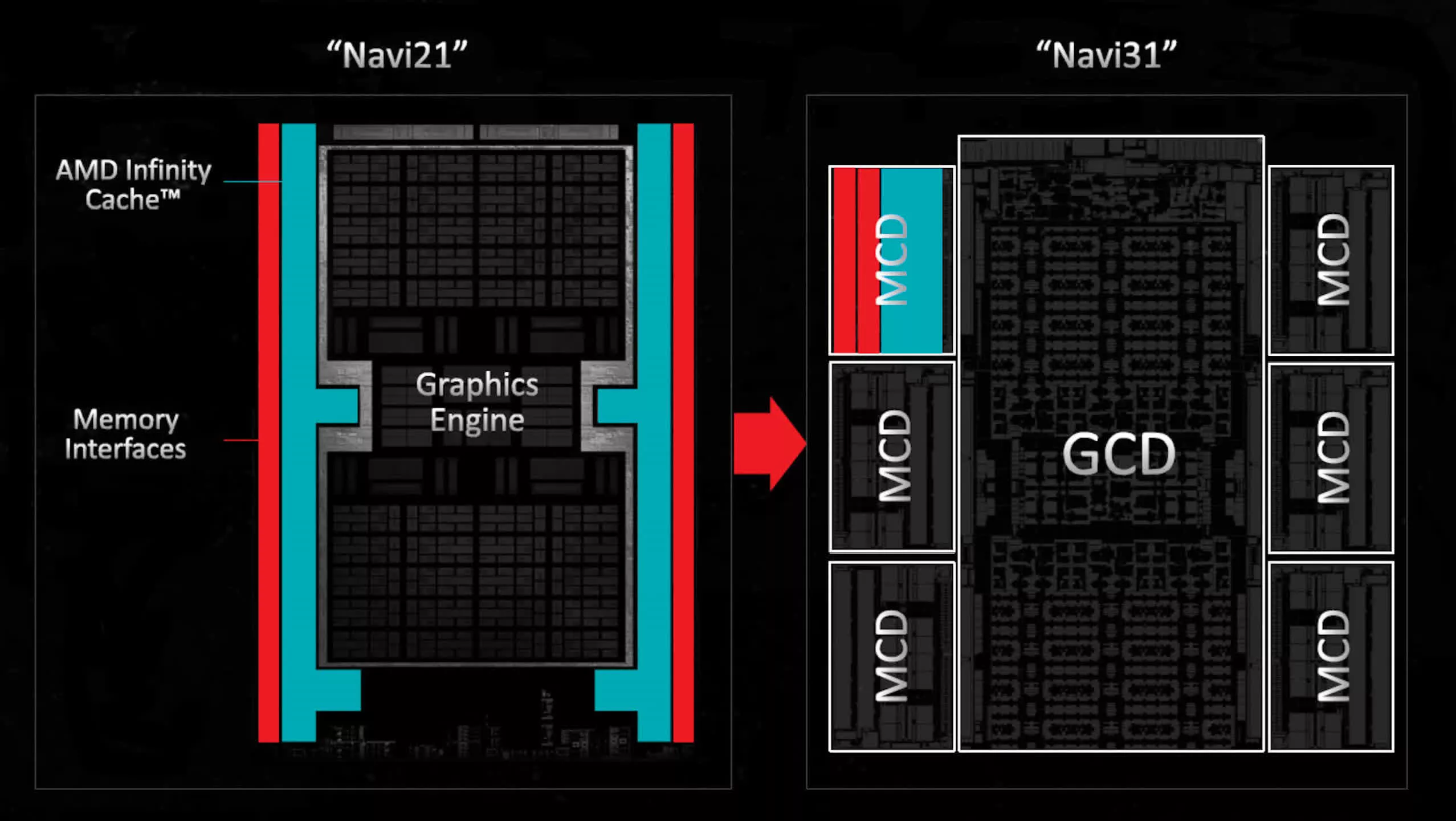
We’ll take a more detailed look at this later in the article, so for now, let’s just concentrate on what parts are where. In the Navi 31, the memory controllers and their associated partitions of the final-tier cache are housed in separate chiplets (called MCDs or Memory Cache Dies) that surround the primary processor (GCD, Graphics Compute Die).
With a greater number of SEs to feed, AMD increased the MC count by 50%, too, so the total bus width to the GDDR6 global memory is now 384-bits. There’s less Infinity Cache in total this time (96MB vs 128MB), but the greater memory bandwidth offsets this.
Intel ACM-G10
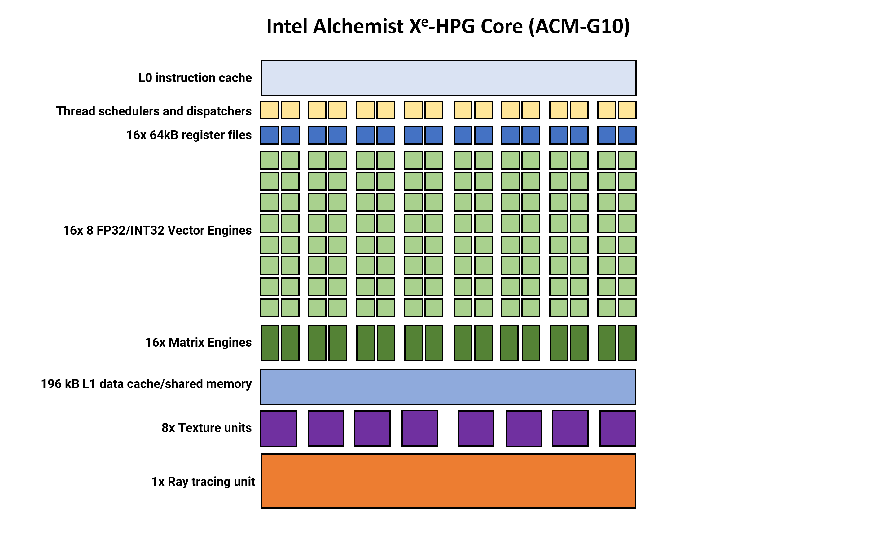
Onward to Intel and the ACM-G10 die (previously called DG2-512). While this isn’t the largest GPU that Intel makes, it’s their biggest consumer graphics die.
The block diagram is a fairly standard arrangement, though looking more akin to Nvidia’s than AMD’s. With a total of 8 Render Slices, each containing 4 Xe-Cores, for a total count of 512 Vector Engines (Intel’s equivalent of AMD’s Stream Processors and Nvidia’s CUDA cores).
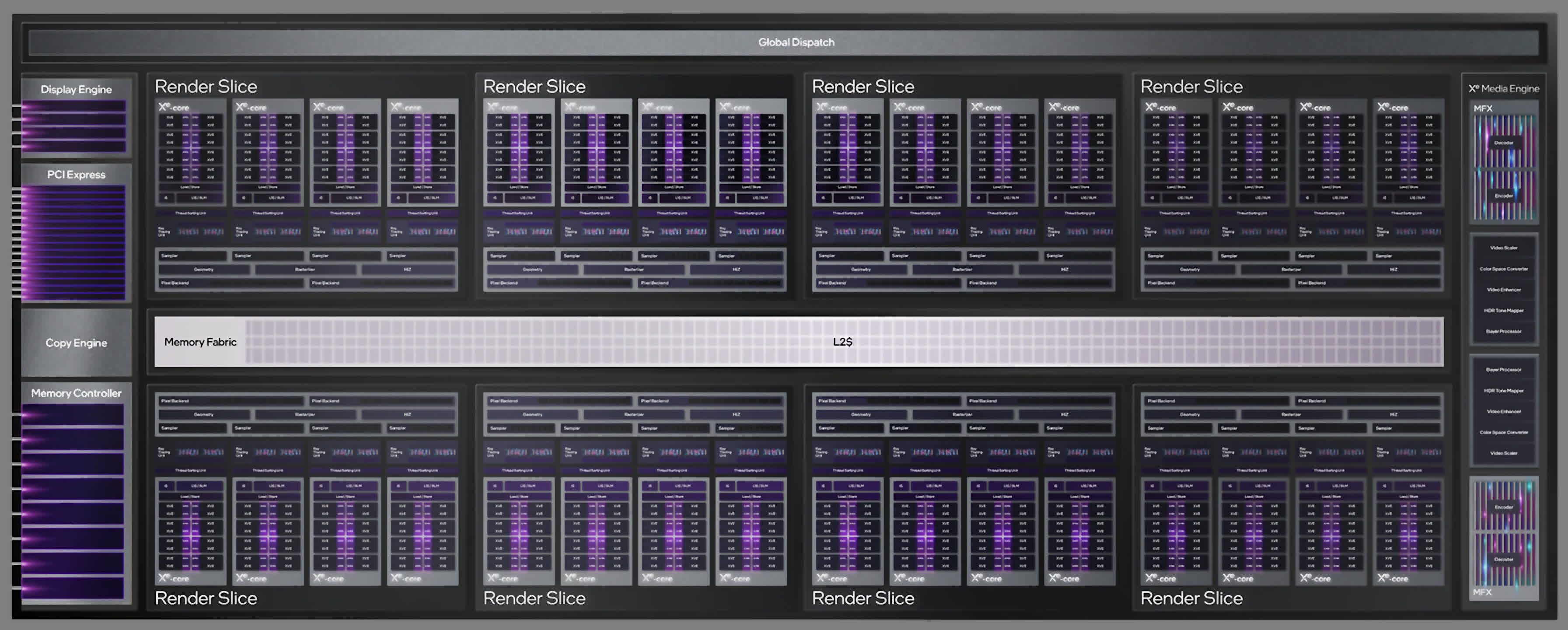
Also packed into each Render Slice is a primitive unit, rasterizer, depth buffer processor, 32 texture units, and 16 ROPs. At first glance, this GPU would appear to be pretty large, as 256 TMUs and 128 ROPs are more than that found in a Radeon RX 6800 or GeForce RTX 2080, for example.
However, AMD’s RNDA 3 chip houses 96 Compute Units, each with 128 ALUs, whereas the ACM-G10’s sports a total of 32 Xe Cores, with 128 ALUs per core. So, in terms of ALU count only, Intel’s Alchemist-powered GPU is a third the size of AMD’s. But as we’ll see later, a significant amount of the ACM-G10’s die is given over to a different number-crunching unit.
Compared to the first Alchemist GPU that Intel released via OEM suppliers, this chip has all the hallmarks of a mature architecture, in terms of component count and structural arrangement.
Nvidia AD102
We finish our opening overview of the different layouts with Nvidia’s AD102, their first GPU to use the Ada Lovelace architecture. Compared to its predecessor, the Ampere GA102, it doesn’t seem all that different, just a lot larger. And to all intents and purposes, it is.
Nvidia uses a component hierarchy of a Graphics Processing Cluster (GPU) that contains 6 Texture Processing Clusters (TPCs), with each of those housing 2 Streaming Multiprocessors (SMs). This arrangement hasn’t changed with Ada, but the total numbers certainly have…
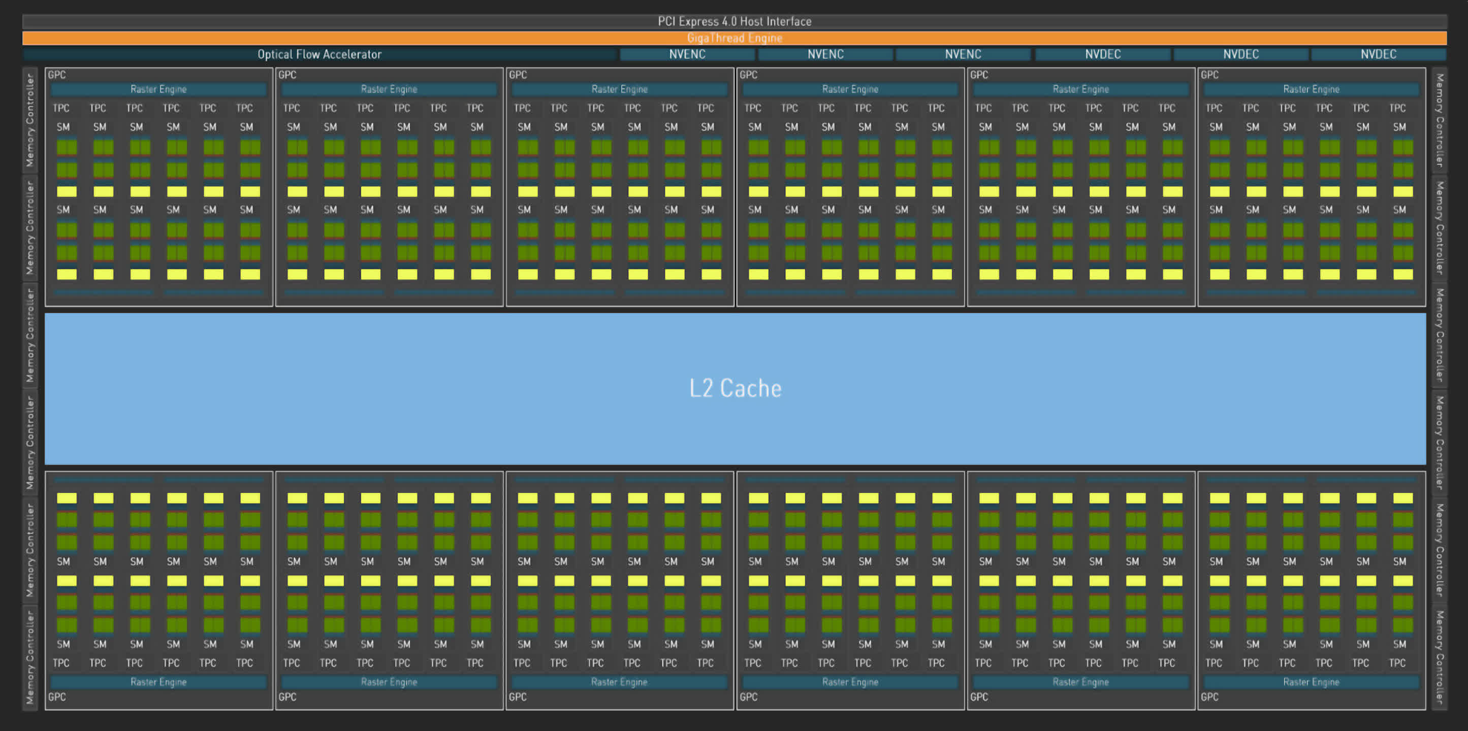
In the full AD102 die, the GPC count has gone from 7 to 12, so there is now a total of 144 SMs, giving a total of 18432 CUDA cores. This might seem like a ridiculously high number when compared to the 6144 SPs in Navi 31, but AMD and Nvidia count their components differently.
Although this is grossly simplifying matters, one Nvidia SM is equivalent to one AMD CU — both contain 128 ALUs. So where Navi 31 is twice the size of the Intel ACM-G10 (ALU count only), the AD102 is 3.5 times larger.
This is why it’s unfair to do any outright performance comparisons of the chips when they’re so clearly different in terms of scale. However, once they’re inside a graphics card, priced and marketed, then it’s a different story.
But what we can compare are the smallest repeated parts of the three processors.
Shader Cores: Into the Brains of the GPU
From the overview of the whole processor, let’s now dive into the hearts of the chips, and look at the fundamental number-crunching parts of the processors: the shader cores.
The three manufacturers use different terms and phrases when it comes to describing their chips, especially when it comes to their overview diagrams. So for this article, we’re going to use our own images, with common colors and structures, so that it’s easier to see what’s the same and what’s different.
AMD RDNA 3
AMD’s smallest unified structure within the shading part of the GPU is called a Double Compute Unit (DCU). In some documents, it’s still called a Workgroup Processor (WGP), whereas others refer to it as a Compute Unit Pair.
Please note that if something isn’t shown in these diagrams (e.g. constants caches, double precision units) that doesn’t mean they’re not present in the architecture.
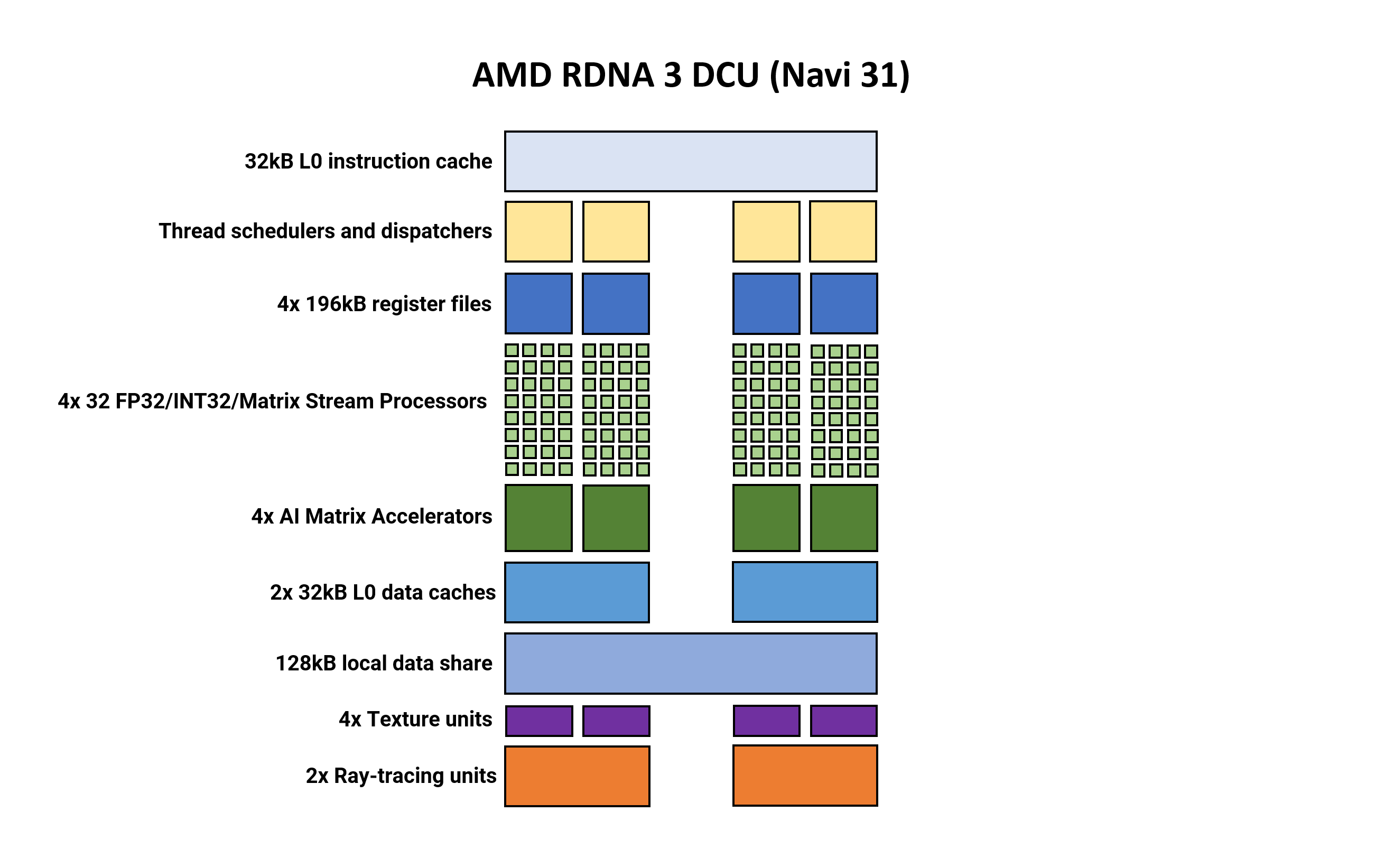
In many ways, the overall layout and structural elements haven’t changed much from RDNA 2. Two Compute Units share some caches and memory, and each one comprises two sets of 32 Stream Processors (SP).
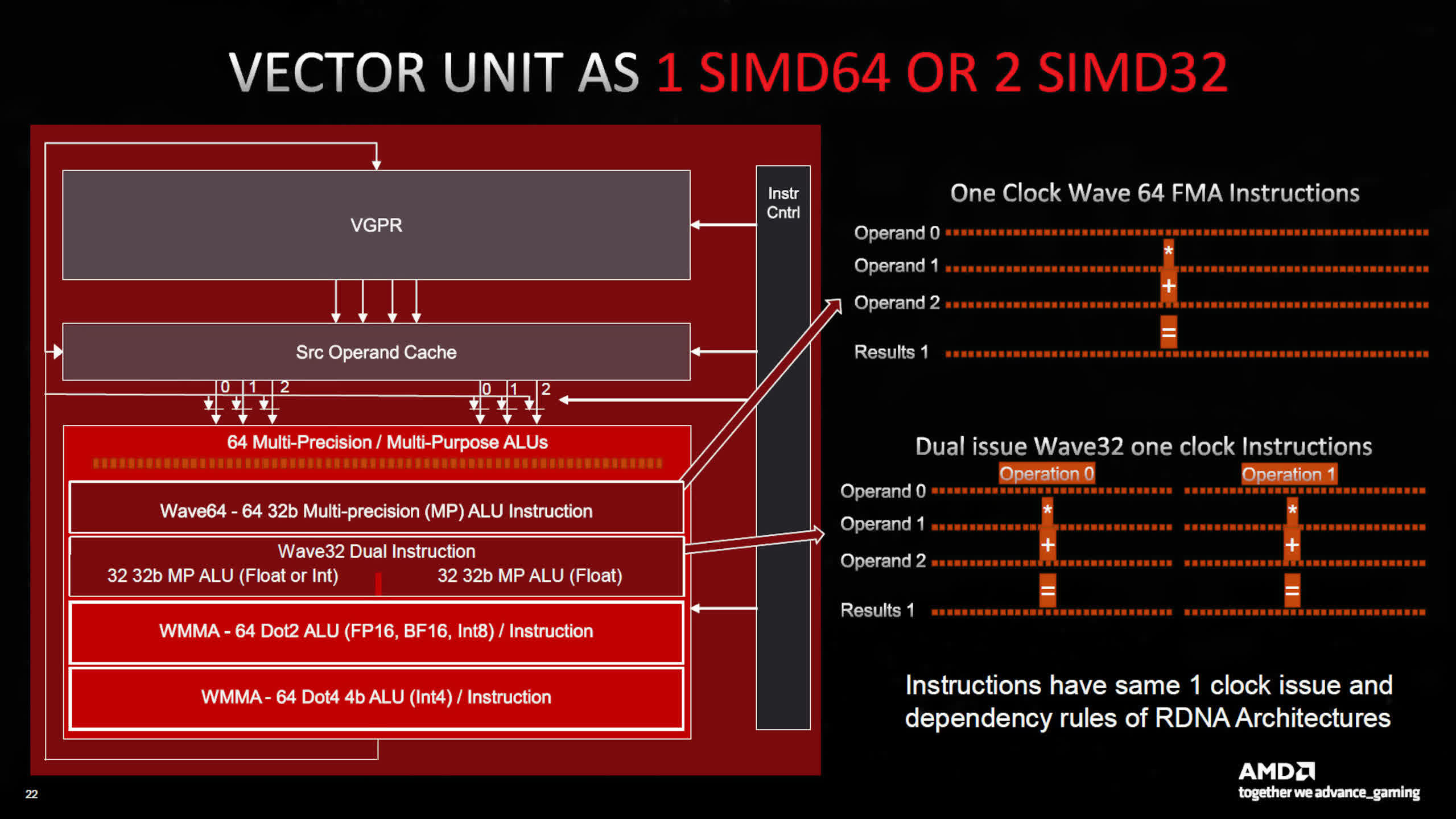
What’s new for version 3, is that each SP now houses twice as many arithmetic logic units (ALUs) as before. There are now two banks of SIMD64 units per CU and each bank has two dataports — one for floating point, integer, and matrix operations, with the other for just float and matrix.
AMD does use separate SPs for different data formats — the Compute Units in RDNA 3 supports operation using FP16, BF16, FP32, FP64, INT4, INT8, INT16, and INT32 values.
The use of SIMD64 means that each thread scheduler can send out a group of 64 threads (called a wavefront), or it can co-issue two wavefronts of 32 threads, per clock cycle. AMD has retained the same instruction rules from previous RDNA architectures, so this is something that’s handled by the GPU/drivers.
Another significant new feature is the appearance of what AMD calls AI Matrix Accelerators.
Unlike Intel’s and Nvidia’s architecture, which we’ll see shortly, these don’t act as separate units — all matrix operations utilize the SIMD units and any such calculations (called Wave Matrix Multiply Accumulate, WMMA) will use the full bank of 64 ALUs.
At the time of writing, the exact nature of the AI Accelerators isn’t clear, but it’s probably just circuitry associated with handling the instructions and the huge amount of data involved, to ensure maximum throughput. It may well have a similar function to that of Nvidia’s Tensor Memory Accelerator, in their Hopper architecture.
Compared to RDNA 2, the changes are relatively small — the older architecture could also handle 64 thread wavefronts (aka Wave64), but these were issued over two cycles and used both SIMD32 blocks in each Compute Unit. Now, this can all be done in one cycle and will only use one SIMD block.
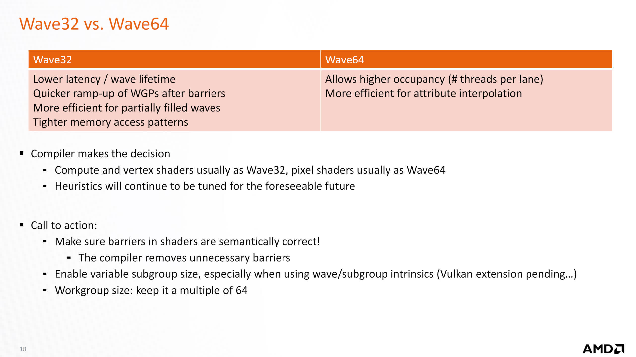
In previous documentation, AMD stated that Wave32 was typically used for compute and vertex shaders (and probably ray shaders, too), whereas Wave 64 was mostly for pixel shaders, with the drivers compiling shaders accordingly. So the move to single cycle Wave64 instruction issue will provide a boost to games that are heavily dependent on pixel shaders.
However, all of this extra power on tap needs to be correctly utilized in order to take full advantage of it. This is something that’s true of all GPU architectures and they all need to be heavily loaded with lots of threads, in order to do this (it also helps hide the inherent latency that’s associated with DRAM).
So with doubling the ALUs, AMD has pushed the need for programmers to use instruction-level parallelism as much as possible. This isn’t something new in the world of graphics, but one significant advantage that RDNA had over AMD’s old GCN architecture was that it didn’t need as many threads in flight to reach full utilization. Given how complex modern rendering has become in games, developers are going to have a little more work on their hands, when it comes to writing their shader code.
Intel Alchemist
Let’s move on to Intel now, and look at the DCU-equivalent in the Alchemist architecture, called an Xe Core (which we’ll abbreviate to XEC). At first glance, these look absolutely huge in comparison to AMD’s structure.
Where a single DCU in RDNA 3 houses four SIMD64 blocks, Intel’s XEC contains sixteen SIMD8 units, each one managed by its own thread scheduler and dispatch system. Like AMD’s Streaming Processors, the so-called Vector Engines in Alchemist can handle integer and float data formats. There’s no support for FP64, but this isn’t much of an issue in gaming.
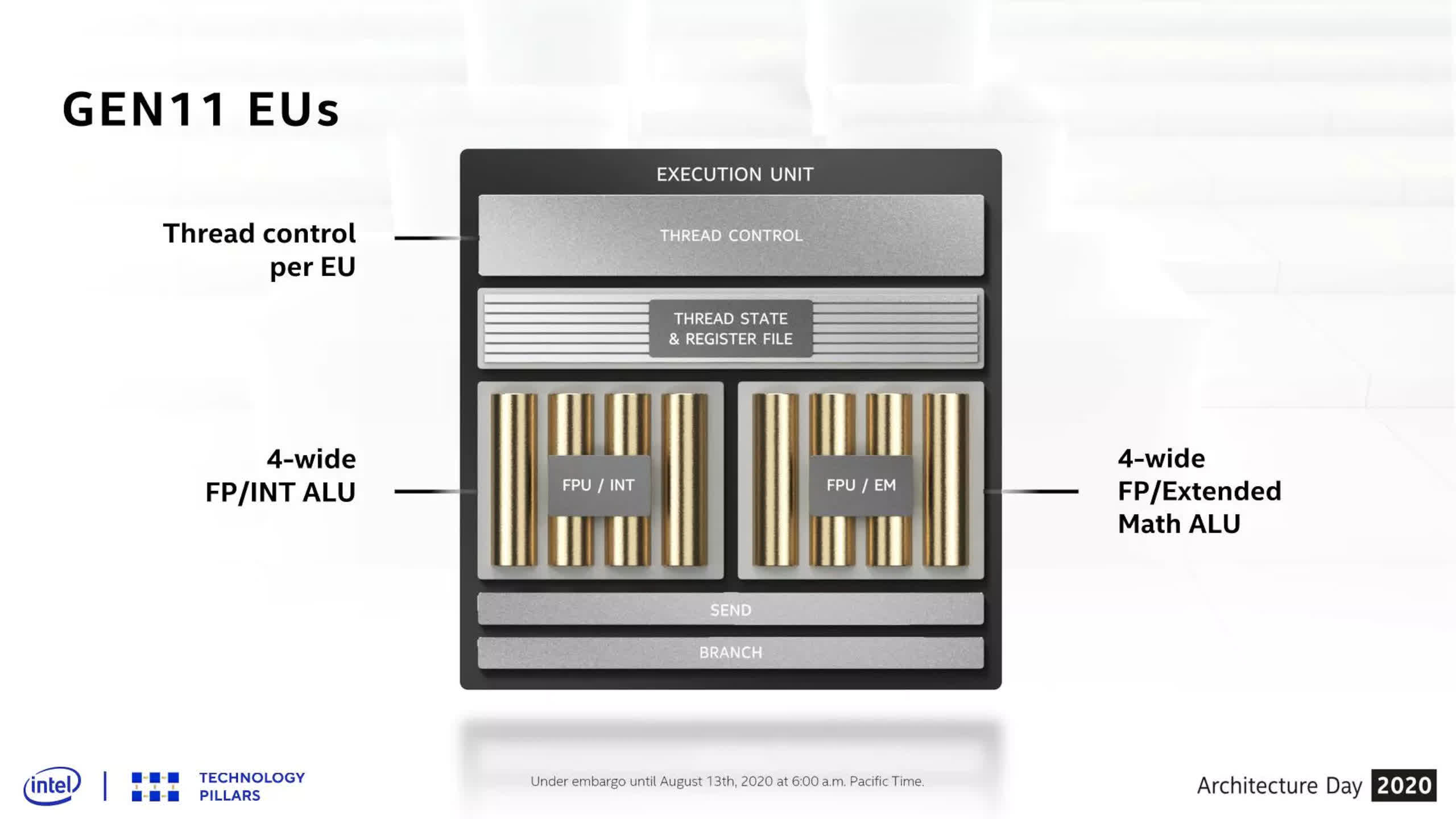
Intel has always used relatively narrow SIMDs — those used in likes of Gen11 were only 4-wide (i.e. handle 4 threads simultaneously) and only doubled in width with Gen 12 (as used in their Rocket Lake CPUs, for example).
But given that the gaming industry has been used to SIMD32 GPUs for a good number of years, and thus games are coded accordingly, the decision to keep the narrow execution blocks seems counter-productive.
Where AMD’s RDNA 3 and Nvidia’s Ada Lovelace have processing blocks that can be issued 64 or 32 threads in a single cycle, Intel’s architecture requires 4 cycles to achieve the same result on one VE — hence why there are sixteen SIMD units per XEC.
However, this means that if games aren’t coded in such a way to ensure the VEs are fully occupied, the SIMDs and associated resources (cache, bandwidth, etc.) will be left idle. A common theme in benchmark results with Intel’s Arc-series of graphics cards is that they tend to do better at higher resolutions and/or in games with lots of complex, modern shader routines.
This is in part due to the high level of unit subdivision and resource sharing that takes place. Micro-benchmarking analysis by website Chips and Cheese shows that for all its wealth of ALUs, the architecture struggles to achieve proper utilization.
Moving on to other aspects in the XEC, it’s not clear how large the Level 0 instruction cache is but where AMD’s are 4-way (because it serves four SIMD blocks), Intel’s will have to be 16-way, which adds to the complexity of the cache system.
Intel also chose to provide the processor with dedicated units for matrix operations, one for each Vector Engine. Having this many units means a significant portion of the die is dedicated to handling matrix math.
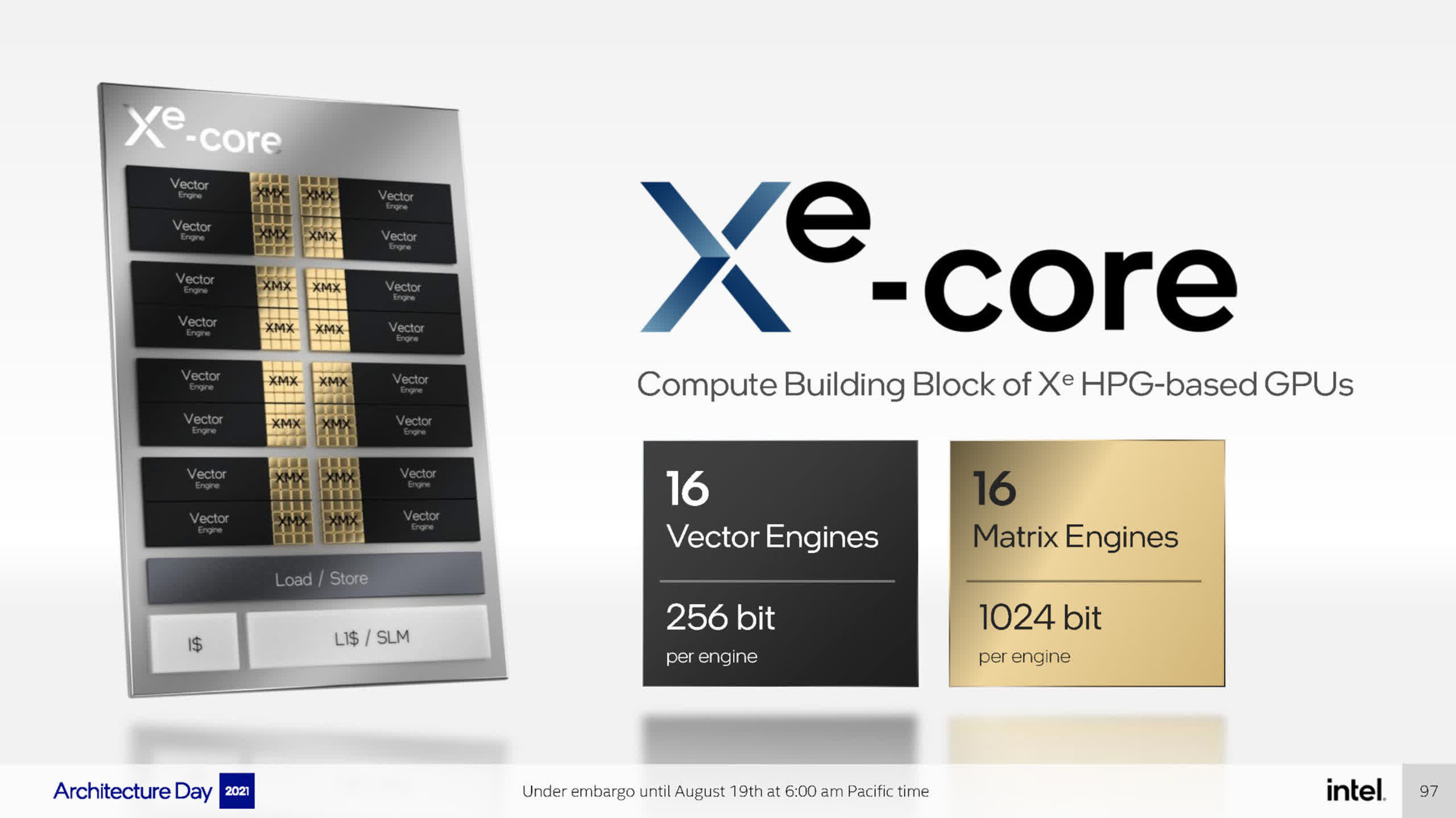
Where AMD uses the DCU’s SIMD units to do this and Nvidia has four relatively large tensor/matrix units per SM, Intel’s approach seems a little excessive, given that they have a separate architecture, called Xe-HP, for compute applications.
Another odd design seems to be the load/store (LD/ST) units in the processing block. Not shown in our diagrams, these manage memory instructions from threads, moving data between the register file and the L1 cache. Ada Lovelace is identical to Ampere with four per SM partition, giving 16 in total. RDNA 3 is also the same as its predecessor, with each CU having dedicated LD/ST circuitry as part of the texture unit.
Intel’s Xe-HPG presentation shows just one LD/ST per XEC but in reality, it’s probably composed of further discrete units inside. However, in their optimization guide for OneAPI, a diagram suggests that the LD/ST cycles through the individual register files one at a time. If that’s the case, then Alchemist will always struggle to achieve maximum cache bandwidth efficiency, because not all files are being served at the same time.
Nvidia Ada Lovelace
The last processing block to look at is Nvidia’s Streaming Multiprocessor (SM) — the GeForce version of the DCU/XEC. This structure hasn’t changed a great deal from the 2018 Turing architecture. In fact, it’s almost identical to Ampere.
Some of the units have been tweaked to improve their performance or feature set, but for the most part, there’s not a great deal that’s new to talk about. Actually, there could be, but Nvidia is notoriously shy at revealing much about the inner operations and specifications of their chips. Intel provides a little more detail, but the information is typically buried in other documents.
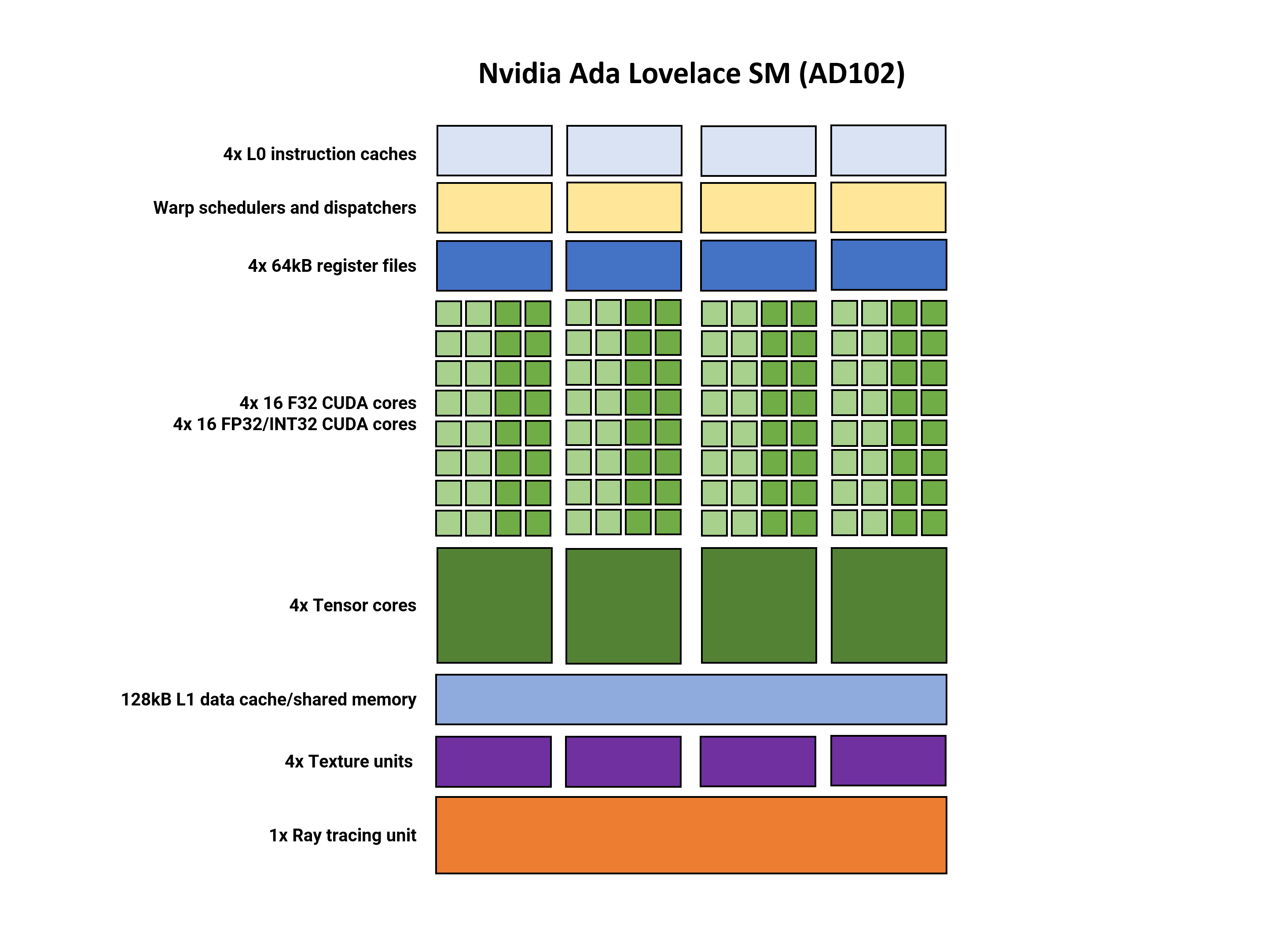
But to summarize the structure, the SM is split into four partitions. Each one has its own L0 instruction cache, thread scheduler and dispatch unit, and a 64 kB section of the register file paired to a SIMD32 processor.
Just as in AMD’s RDNA 3, the SM supports dual-issued instructions, where each partition can concurrently process two threads, one with FP32 instructions and the other with FP32 or INT32 instructions.
Nvidia’s Tensor cores are now in their 4th revision but this time, the only notable change was the inclusion of the FP8 Transformer Engine from their Hopper chip — raw throughput figures remain unaltered.
The addition of the low-precision float format means that the GPU should be more suitable for AI training models. The Tensor cores still also offer the sparsity feature from Ampere, which can provide up to double the throughput.
Another improvement lies in the Optical Flow Accelerator (OFA) engine (not shown in our diagrams). This circuit generates an optical flow field, which is used as part of the DLSS algorithm. With double the performance of the OFA in Ampere, the extra throughput is utilized in the latest version of their temporal, anti-aliasing upscaler, DLSS 3.
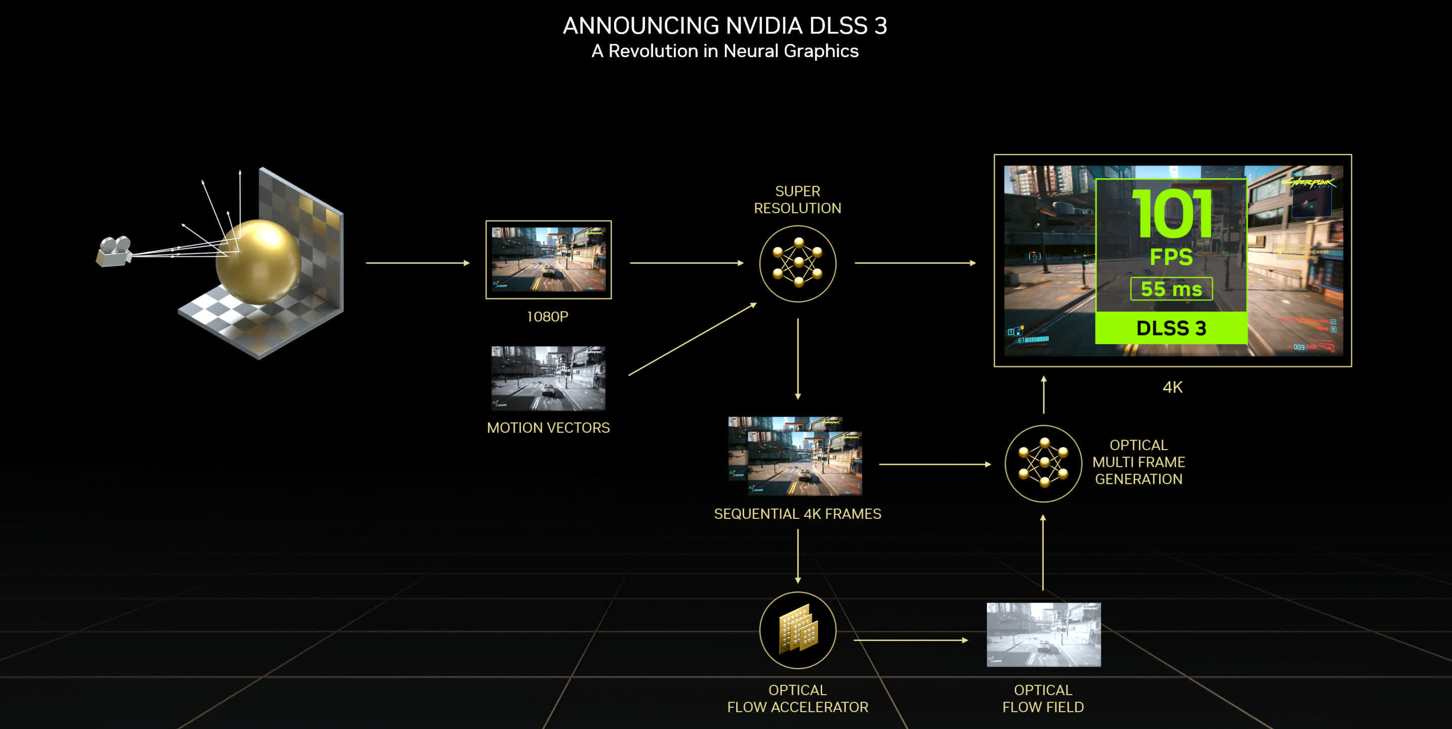
DLSS 3 has already faced a fair amount of criticism, centering around two aspects: the DLSS-generated frames aren’t ‘real’ and the process adds additional latency to the rendering chain. The first isn’t entirely invalid, as the system works by first having the GPU render two consecutive frames, storing them in memory, before using a neural network algorithm to determine what an intermediary frame would look like.
The present chain then returns to the first rendered frame and displays that one, followed by the DLSS-frame, and then the second frame rendered. Because the game’s engine hasn’t cycled for the middle frame, the screen is being refreshed without any potential input. And because the two successive frames need to be stalled, rather than presented, any input that has been polled for those frames will also get stalled.
Whether DLSS 3 ever becomes popular or commonplace remains to be seen.
Although the SM of Ada is very similar to Ampere, there are notable changes to the RT core and we’ll address those shortly. For now, let’s summarize the computational capabilities of AMD, Intel, and Nvidia’s GPU repeated structures.
Processing Block Comparison
We can compare the SM, XEC, and DCU capabilities by looking at the number of operations, for standard data formats, per clock cycle. Note that these are peak figures and are not necessarily achievable in reality.
| Operations per clock | Ada Lovelace | Alchemist | RDNA 3 |
| FP32 | 128 | 128 | 256 |
| FP16 | 128 | 256 | 512 |
| FP64 | 2 | n/a | 16 |
| INT32 | 64 | 128 | 128 |
| FP16 matrix | 512 | 2048 | 256 |
| INT8 matrix | 1024 | 4096 | 256 |
| INT4 matrix | 2048 | 8192 | 1024 |
Nvidia’s figures haven’t changed from Ampere, whereas RDNA 3’s numbers have doubled in some areas. Alchemist, though, is on another level when it comes to matrix operations, although the fact that these are peak theoretical values should be emphasized again.
Given that Intel’s graphics division leans heavily towards data center and compute, just like Nvidia does, it’s not surprising to see the architecture dedicate so much die space to matrix operations. The lack of FP64 capability isn’t a problem, as that data format isn’t really used in gaming, and the functionality is present in their Xe-HP architecture.
Ada Lovelace and Alchemist are, theoretically, stronger than RDNA 3 when it comes to matrix/tensor operations, but since we’re looking at GPUs that are primarily used for gaming workloads, the dedicated units mostly just provide acceleration for algorithms involved in DLSS and XeSS — these use a convolutional auto-encoder neural network (CAENN) that scans an image for artifacts and corrects them.
AMD’s temporal upscaler (FidelityFX Super Resolution, FSR) doesn’t use a CAENN, as it’s based primarily on a Lanczos resampling method, followed by a number of image correction routines, processed via the DCUs. However, in the RDNA 3 launch, the next version of FSR was briefly introduced, citing a new feature called Fluid Motion Frames. With a performance uplift of up to double that of FSR 2.0, the general consensus is that this is likely to involve frame generation, as in DLSS 3, but whether this involves any matrix operations is yet to be clear.
Ray Tracing for Everybody Now
With the launch of their Arc graphics cards series, using the Alchemist architecture, Intel joined AMD and Nvidia in offering GPUs that provided dedicated accelerators for various algorithms involved with the use of ray tracing in graphics. Both Ada and RNDA 3 contain significantly updated RT units, so it makes sense to take a look at what’s new and different.
Starting with AMD, the biggest change to their Ray Accelerators is adding hardware to improve the traversal of the bounding volume hierarchies (BVH). These are data structures that are used to speed up determining what surface a ray of light has hit, in the 3D world.
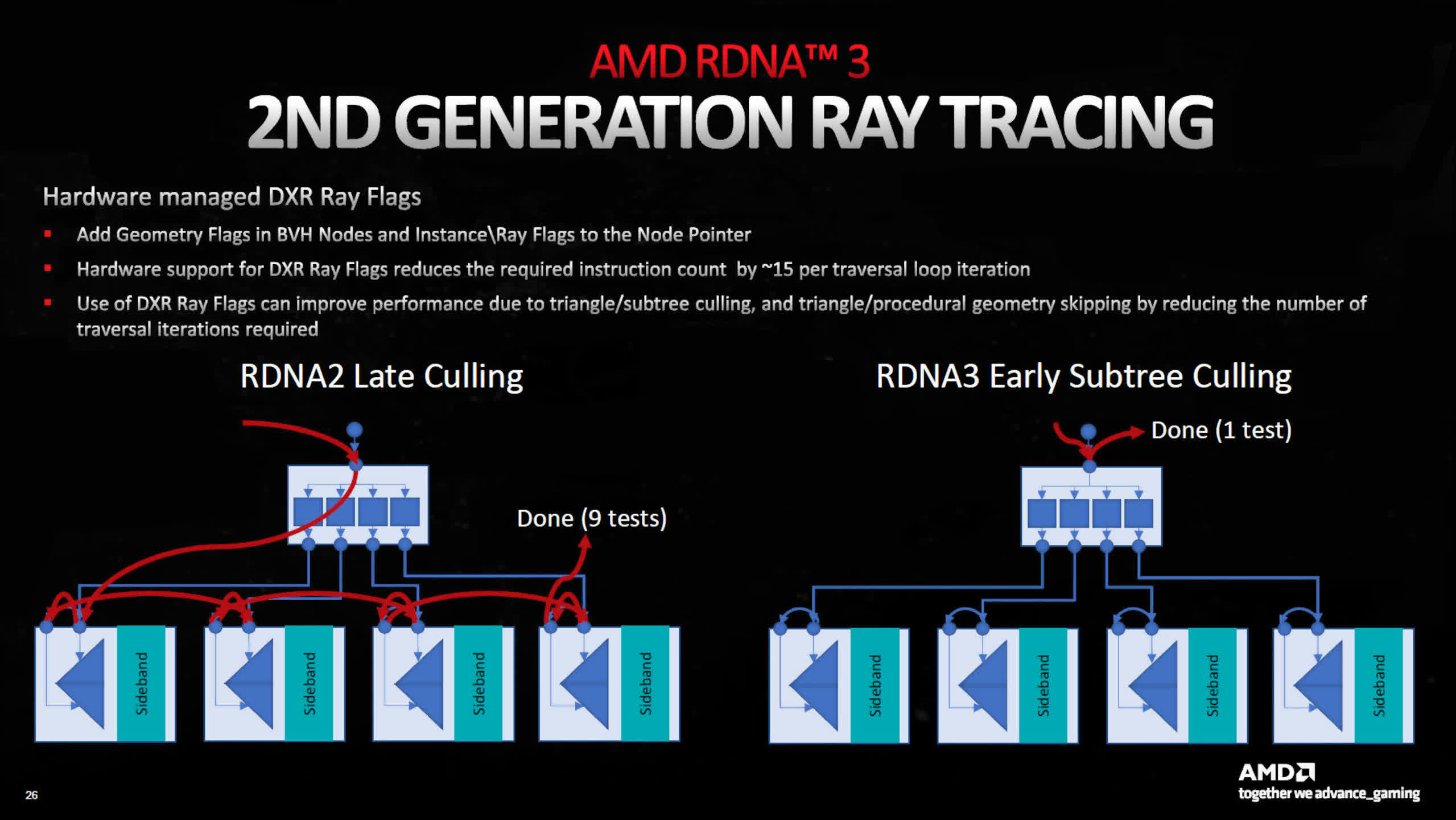
In RDNA 2, all of this work was processed via the Compute Units, and to a certain extent, it still is. However, for DXR, Microsoft’s ray tracing API, there’s hardware support for the management of ray flags.
The use of these can greatly reduce the number of times the BVH needs to be traversed, reducing the overall load on cache bandwidth and compute units. In essence, AMD has focused on improving the overall efficiency of the system they introduced in the previous architecture.
Additionally, the hardware has been updated to improve box sorting (which makes traversal faster) and culling algorithms (to skip testing empty boxes). Coupled with improvements to the cache system, AMD states that there’s up to 80% more ray tracing performance, at the same clock speed, compared to RDNA 2.
However, such improvements do not translate into 80% more frames per second in games using ray tracing — the performance in these situations is governed by many factors and the capabilities of the RT units is just one of them.
With Intel being new to the ray tracing game, there are no improvements as such. Instead, we’re simply told that their RT units handle BVH traversal and intersection calculations, between rays and triangles. This makes them more akin to Nvidia’s system than AMD’s, but there’s not a great deal of information available about them.
But we do know that each RT unit has an unspecified-sized cache for storing BVH data and a separate unit for analyzing and sorting ray shader threads, to improve SIMD utilization.
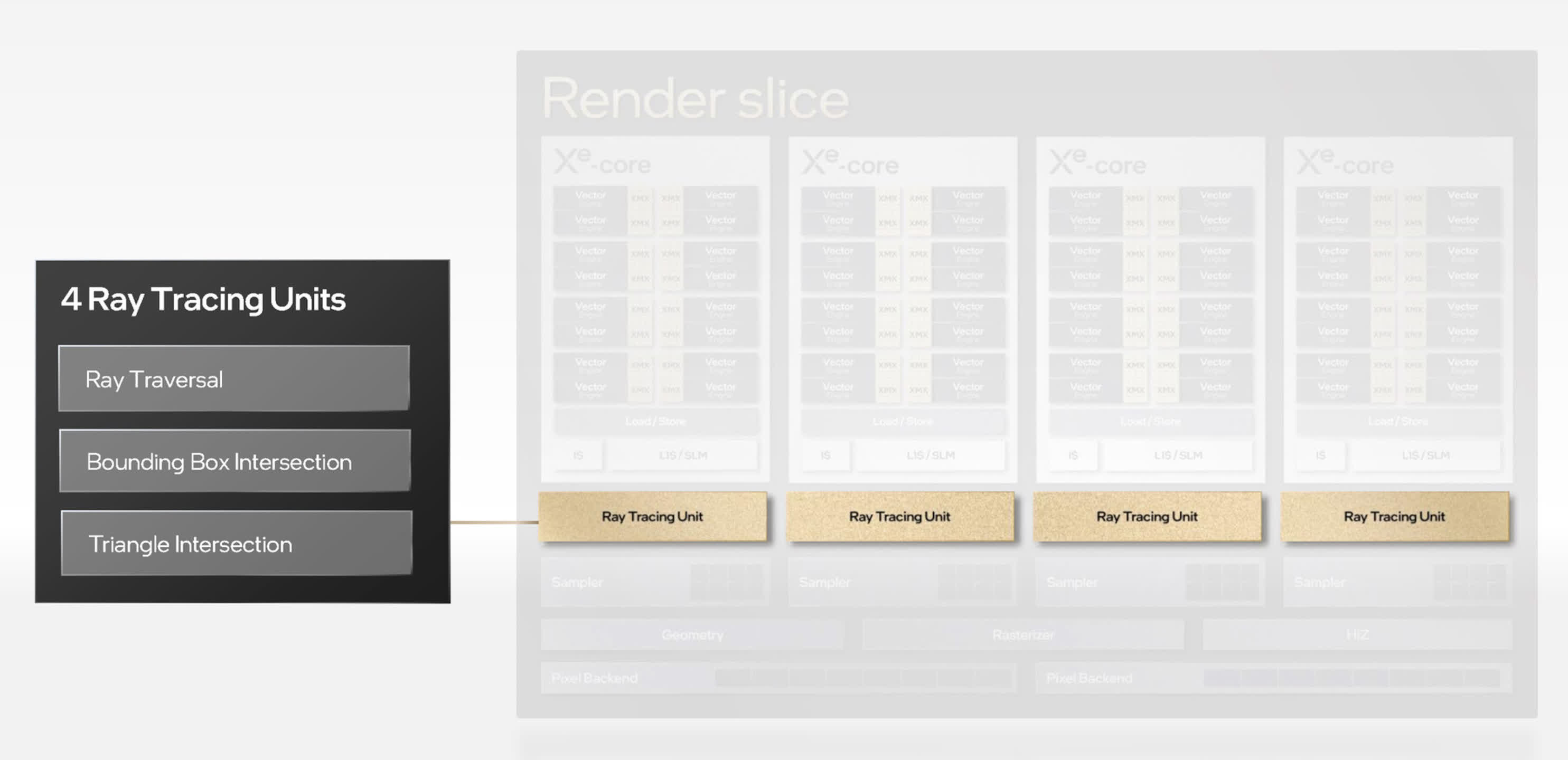
Each XEC is paired with one RT unit, giving a total of four per Render Slice. Some early testing of the A770 with ray tracing enabled in games shows that whatever structures Intel has in place, Alchemist’s overall capability in ray tracing is at least as good as that found with Ampere chips, and a little better than RDNA 2 models.
But let us repeat again that ray tracing also places heavy stress on the shading cores, cache system, and memory bandwidth, so it’s not possible to extract the RT unit performance from such benchmarks.
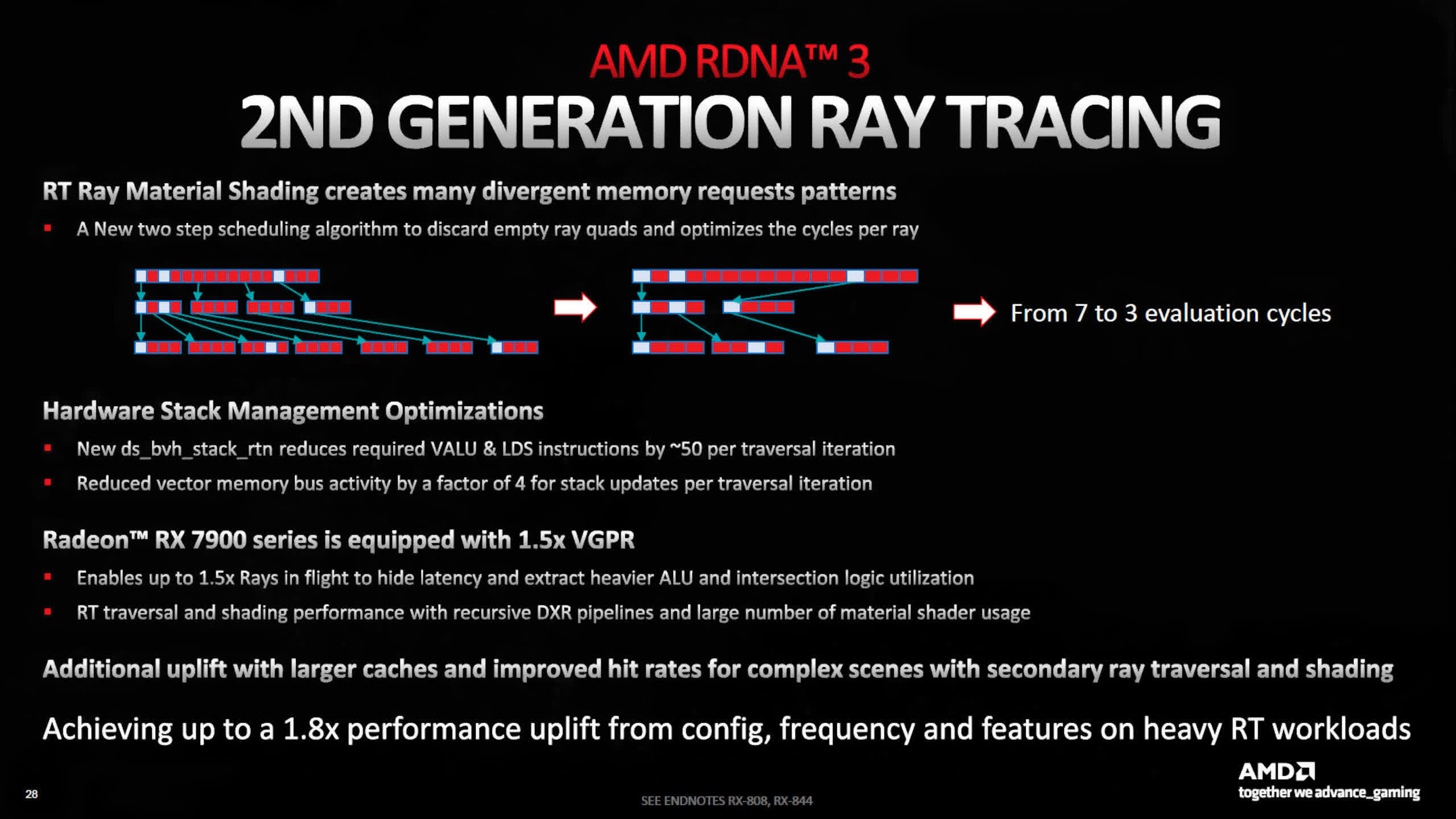
For the Ada Lovelace architecture, Nvidia made a number of changes, with suitably large claims for the performance uplift, compared to Ampere. The accelerators for ray-triangle intersection calculations are claimed to have double the throughput, and BVH traversal for non-opaque surfaces is now said to be twice as fast. The latter is important for objects that use textures with an alpha channel (transparency), for example, leaves on a tree.
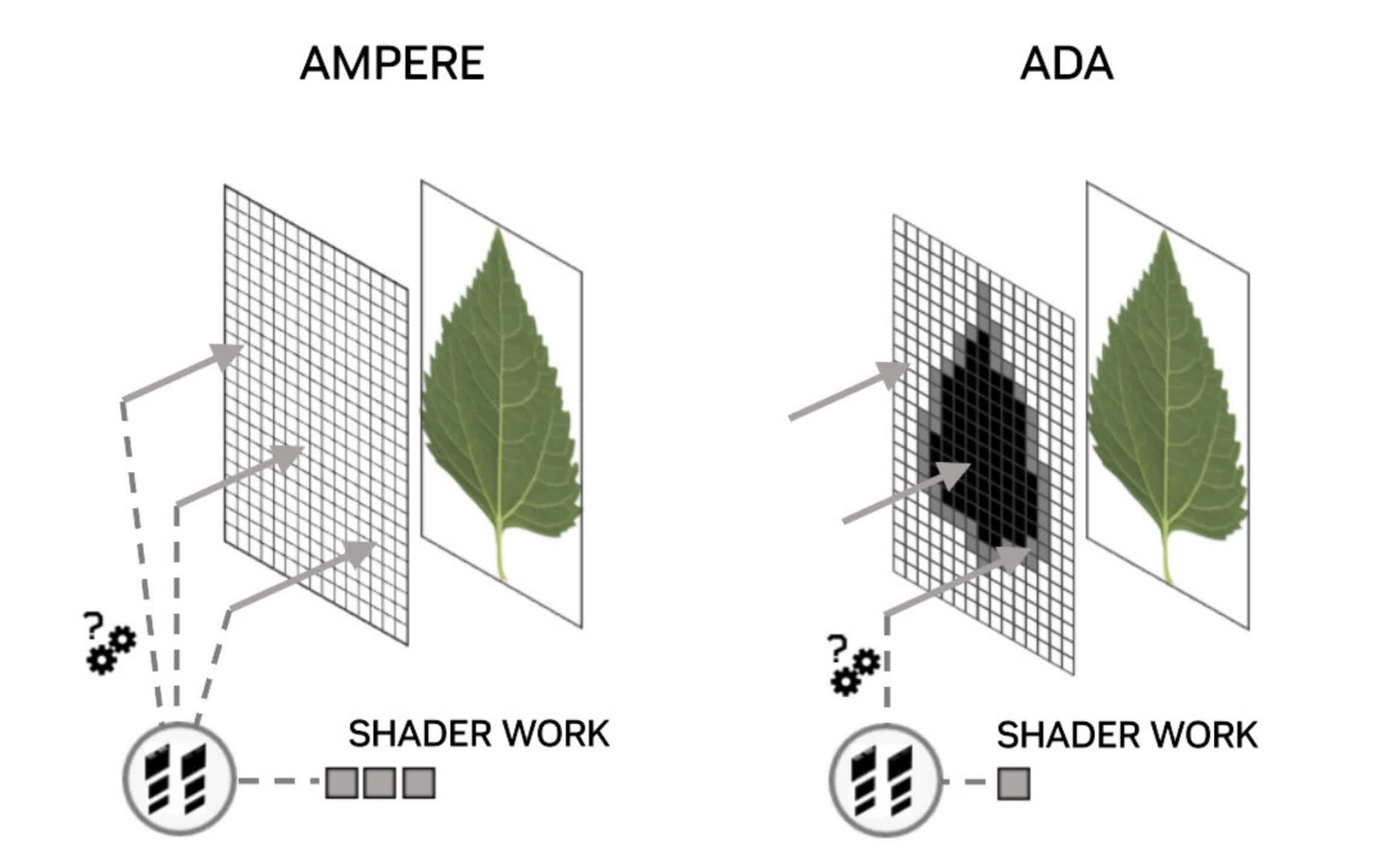
A ray hitting a fully transparent section of such a surface shouldn’t result in a hit result — the ray should pass straight through. However, to accurately determine this in current games with ray tracing, multiple other shaders need to be processed. Nvidia’s new Opacity Micromap Engine breaks up these surfaces into further triangles and then determines what exactly is going on, reducing the number of ray shaders required.
Two further additions to the ray tracing abilities of Ada are a reduction in build time and memory footprint of the BVHs (with claims of 10x faster and 20x smaller, respectively), and a structure to reorder threads for ray shaders, giving better efficiency. However, where the former requires no changes in software by developers, the latter is currently only accessed by an API from Nvidia, so it’s of no benefit to current DirectX 12 games.
When we tested the GeForce RTX 4090’s ray tracing performance, the average drop in frame rate with ray tracing enabled, was just under 45%. With the Ampere-powered GeForce RTX 3090 Ti, the drop was 56%. However, this improvement cannot be exclusively attributed to the RT core improvements, as the 4090 has substantially more shading throughput and cache than the previous model.
We’ve yet to see how what kind of difference RDNA 3’s ray tracing improvements amount to, but it’s worth noting that none of the GPU manufacturers expects RT to be used in isolation — i.e. the use of upscaling is still required to achieve high frame rates.
Fans of ray tracing may be somewhat disappointed that there haven’t been any major gains in this area, with the new round of graphics processors, but a lot of progress has been made from when it first appeared, back in 2018 with Nvidia’s Turing architecture.
Memory: Driving Down the Data Highways
GPUs crunch through data like no other chip and keeping the ALUs fed with numbers is crucial to their performance. In the early days of PC graphics processors, there was barely any cache inside and the global memory (the RAM used by the entire chip) was desperately slow DRAM. Even just 10 years ago, the situation wasn’t that much better.
So let’s dive into what’s the current state of affairs, starting with AMD’s memory hierarchy in their new architecture. Since its first iteration, RDNA has used a complex, multi-level memory hierarchy. The biggest changes came last year when a huge amount of L3 cache was added to the GPU, up to 128MB in certain models.
This is still the case for round three, but with some subtle changes.
The register files are now 50% larger (which they had to be, to cope with the increase in ALUs) and the first three levels of cache are all now larger. L0 and L1 have doubled in size, and the L2 cache is up to 2MB, to a total of 6MB in the Navi 31 die.
The L3 cache has actually shrunk to 96MB, but there’s a good reason for this — it’s no longer in the GPU die. We’ll talk more about that aspect in a later section of this article.
With wider bus widths between the various cache levels, the overall internal bandwidth is a lot higher too. Clock-for-clock, there’s 50% more between L0 and L1, and the same increase between L1 and L2. But the biggest improvement is between L2 and the external L3 — it’s now 2.25 times wider, in total.
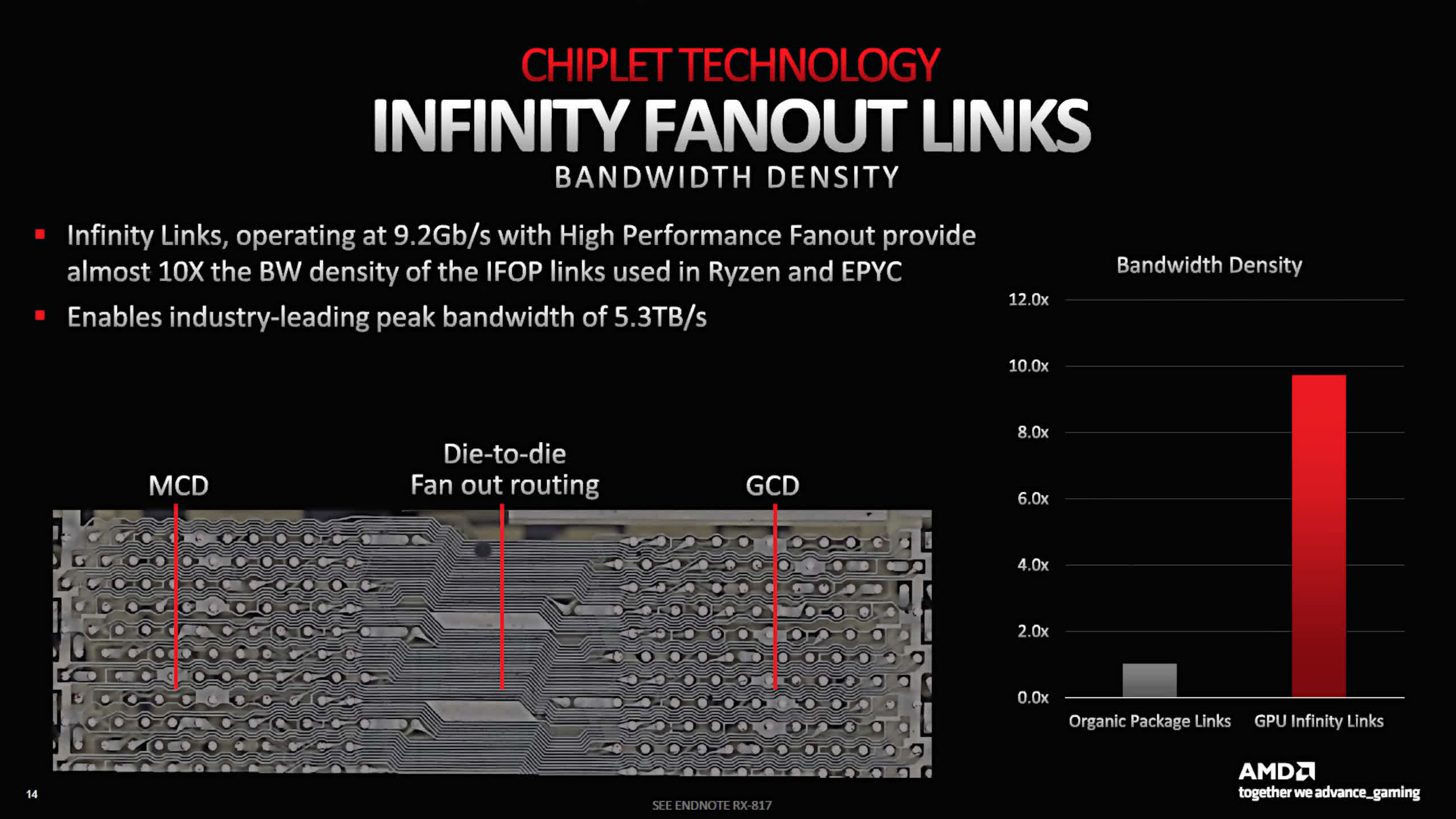
The Navi 21, as used in Radeon RX 6900 XT, had an L2-to-L3 total peak bandwidth of 2.3 TB/s; the Navi 31 in the Radeon RX 7900 XT increases that to 5.3 TB/s, due to the use of AMD’s Infinity fanout links.
Having the L3 cache separate from the main die does increase latency, but this is offset by the use of higher clocks for the Infinity Fabric system — overall, there’s a 10% reduction in L3 latency times compared to RDNA 2.
RDNA 3 is still designed to use GDDR6, rather than the slightly faster GDDR6X, but the top-end Navi 31 chip houses two more memory controllers to increase the global memory bus width to 384 bits.
AMD’s cache system is certainly more complex than Intel’s and Nvidia’s, but micro-benchmarking of RDNA 2 by Chips and Cheese shows that it’s a very efficient system. The latencies are low all around and it provides the background support required for the CUs to reach high utilization, so we can expect the same of the system used in RDNA 3.
Intel’s memory hierarchy is somewhat simpler, being primarily a two-tier system (ignoring smaller caches, such as those for constants). There’s no L0 data cache, just a decent amount 192kB of L1 data & shared memory.
Just as with Nvidia, this cache can be dynamically allocated, with up to 128kB of it being available as shared memory. Additionally, there’s a separate 64kB texture cache (not shown in our diagram).
For a chip (the DG2-512 as used in the A770) that was designed to be used in graphics cards for the mid-range market, the L2 cache is very large at 16MB in total. The data width is suitably big, too, with a total 2048 bytes per clock, between L1 and L2. This cache comprises eight partitions, with each serving a single 32-bit GDDR6 memory controller.
However, analysis has shown that despite the wealth of cache and bandwidth on tap, the Alchemist architecture isn’t particularly good at fully using it all, requiring workloads with high thread counts to mask its relatively poor latency.
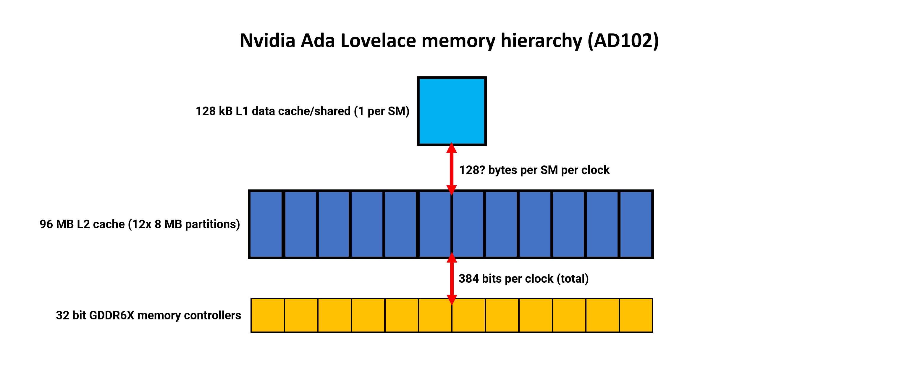
Nvidia has retained the same memory structure as used in Ampere, with each SM sporting 128kB of cache that acts as an L1 data store, shared memory, and texture cache. The amount available for the different roles is dynamically allocated. Nothing has yet been said about any changes to the L1 bandwidth, but in Ampere it was 128 bytes per clock per SM. Nvidia has never been explicitly clear whether this figure is cumulative, combining read and writes, or for one direction only.
If Ada is at least the same as Ampere, then the total L1 bandwidth, for all SMs combined, is an enormous 18 kB per clock — far larger than RDNA 2 and Alchemist.
But it must be stressed again that the chips are not directly comparable, as Intel’s was priced and marketed as a mid-range product, and AMD has made it clear that the Navi 31 was never designed to compete against Nvidia’s AD102. Its competitor is the AD103 which is substantially smaller than the AD102.
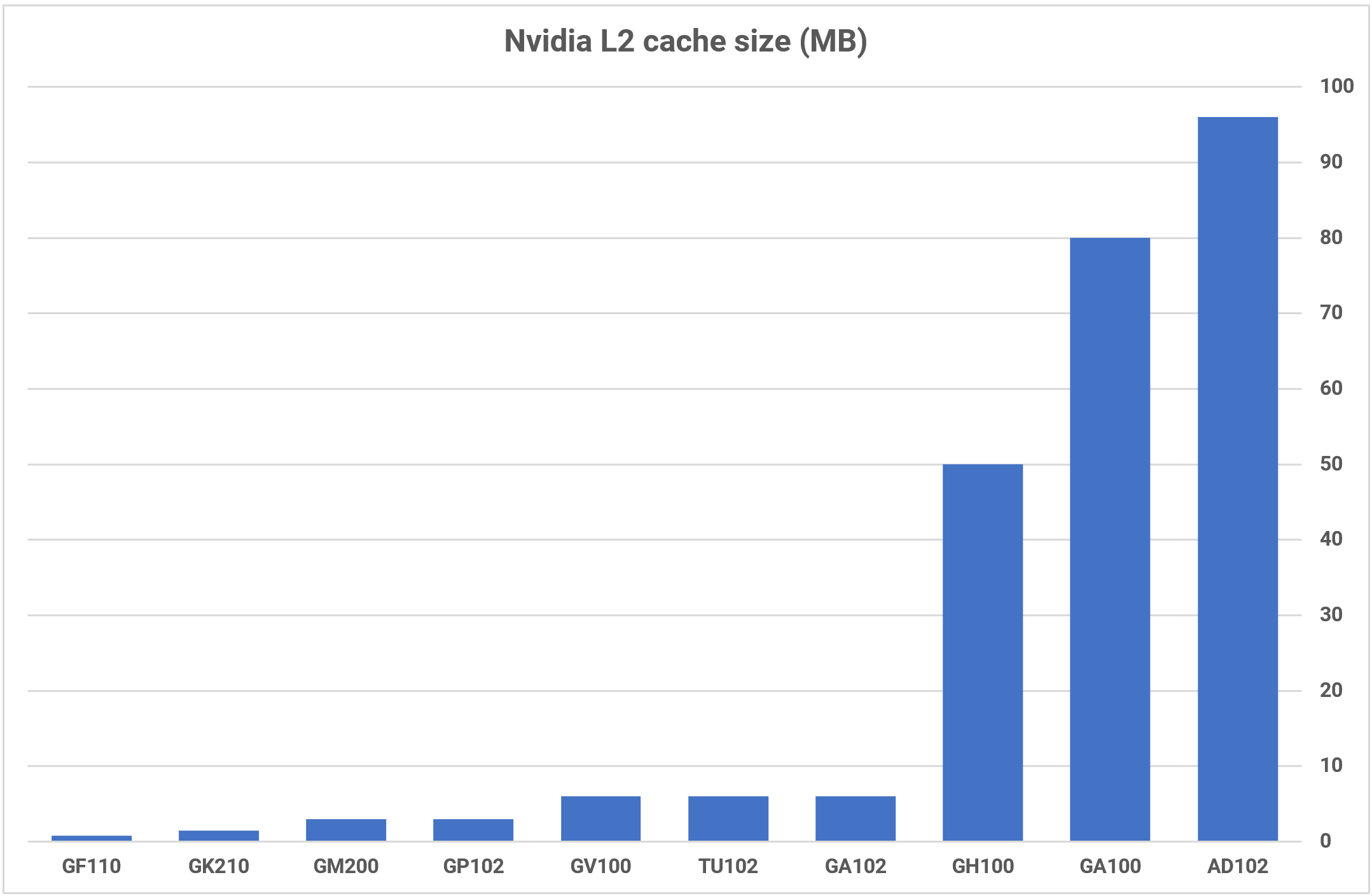
The biggest change to the memory hierarchy is that the L2 cache has ballooned to 96MB, in a full AD102 die — 16 times more than its predecessor, the GA102. As with Intel’s system, the L2 is partitioned and paired with a 32-bit GDDR6X memory controller, for a DRAM bus width of up to 384 bits.
Larger cache sizes typically have longer latencies than smaller ones, but due to increased clock speeds and some improvements with the buses, Ada Lovelace displays better cache performance than Ampere.
If we compare all three systems, Intel and Nvidia take the same approach for the L1 cache — it can be used as a read-only data cache or as a compute shared memory. In the case of the latter, the GPUs need to be explicitly instructed, via software, to use it in this format and the data is only retained for as long as the threads using it are active. This adds to the system’s complexity, but it produces a useful boost to compute performance.
In RDNA 3, the ‘L1’ data cache and shared memory are separated into two 32kB L0 vector caches and a 128kB local data share. What AMD calls L1 cache is really a shared stepping stone, for read-only data, between a group of four DCUs and the L2 cache.
While none of the cache bandwidths are as high as Nvidia’s, the multi-tiered approach helps to counter this, especially when the DCUs aren’t fully utilized.
Enormous, processor-wide cache systems aren’t generally the best for GPUs, which is why we’ve not seen much more than 4 or 6MB in previous architectures, but the reason why AMD, Intel, and Nvidia all have substantial amounts in the final tier is to counter the relative lack of growth in DRAM speeds.
Adding lots of memory controllers to a GPU can provide plenty of bandwidth, but at the cost of increased die sizes and manufacturing overheads, and alternatives such as HBM3 are a lot more expensive to use.
We’ve yet to see how well AMD’s system ultimately performs but their four-tiered approach in RDNA 2 fared well against Ampere, and it’s substantially better than Intel’s. However, with Ada packing in considerably more L2, the competition is no longer as straightforward.
Chip Packaging and Process Nodes: Different Ways to Build a Power Plant
There’s one thing that AMD, Intel, and Nvidia all have in common — they all use TSMC to fabricate their GPUs.
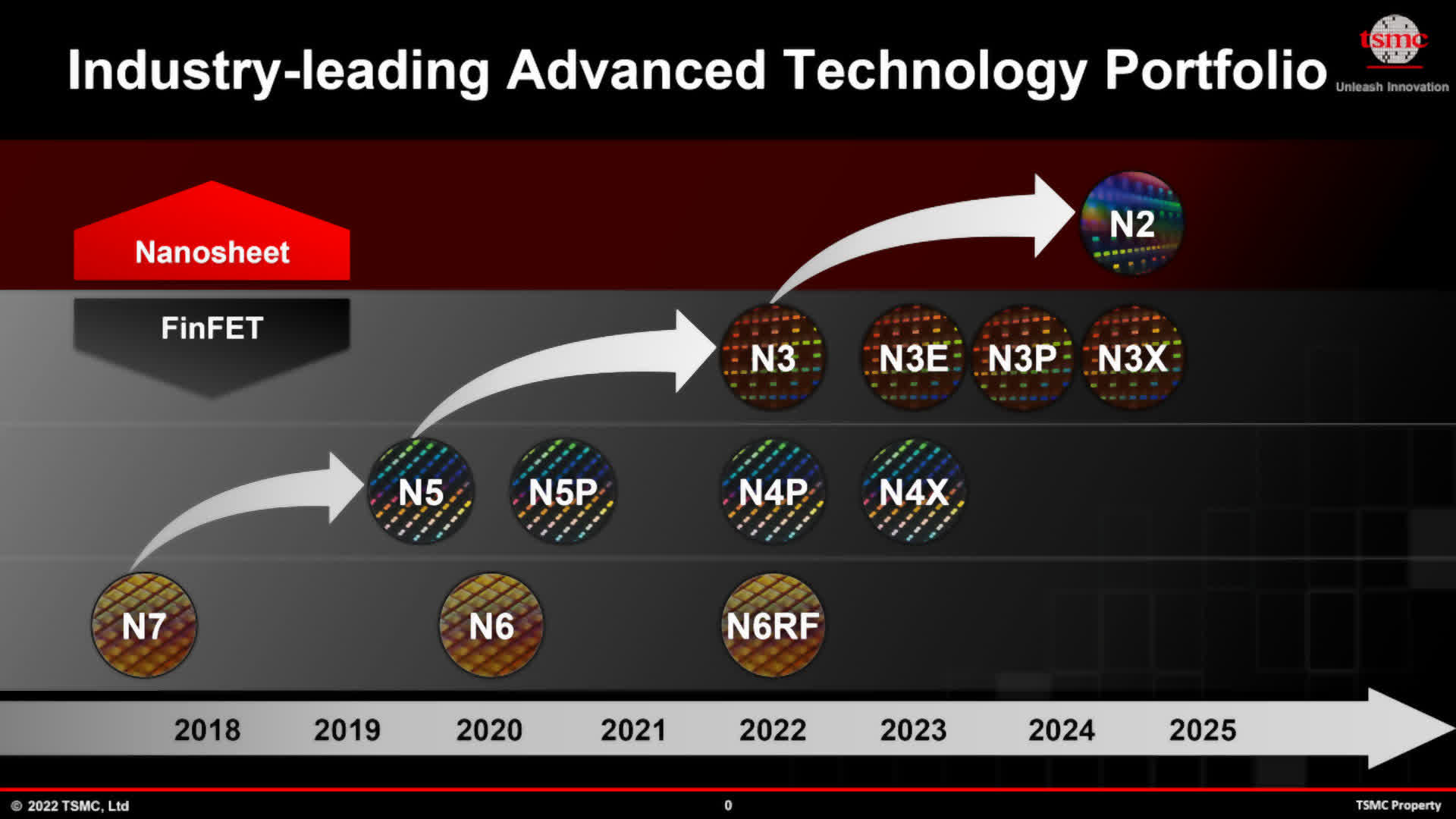
AMD uses two different nodes for the GCD and MCDs in Navi 31, with the former made using the N5 node and the latter on N6 (an enhanced version of N7). Intel also uses N6 for all its Alchemist chips. With Ampere, Nvidia used Samsung’s old 8nm process, but with Ada they switched back to TSMC and its N4 process, which is a variant of N5.
N4 has the highest transistor density and the best performance-to-power ratio of all the nodes, but when AMD launched RDNA 3, they highlighted that only logic circuitry has seen any notable increase in density.
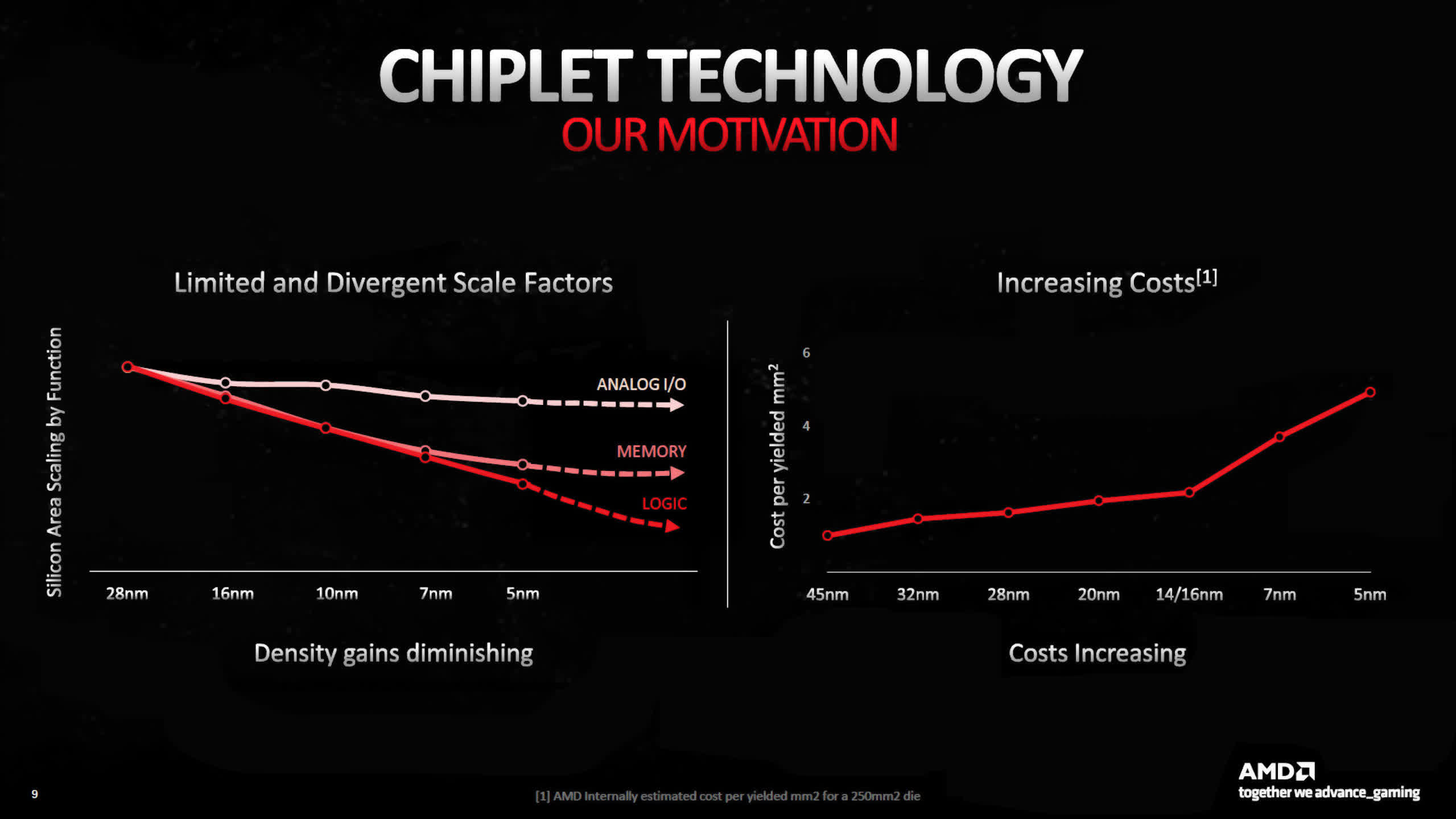
SRAM (used for cache) and analog systems (used for memory, system, and other signaling circuits) have shrunk relatively little. Coupled with the rise in price per wafer for the newer process nodes, AMD made the decision to use the slightly older and cheaper N6 to fabricate the MCDs, as these chiplets are mostly SRAM and I/O.
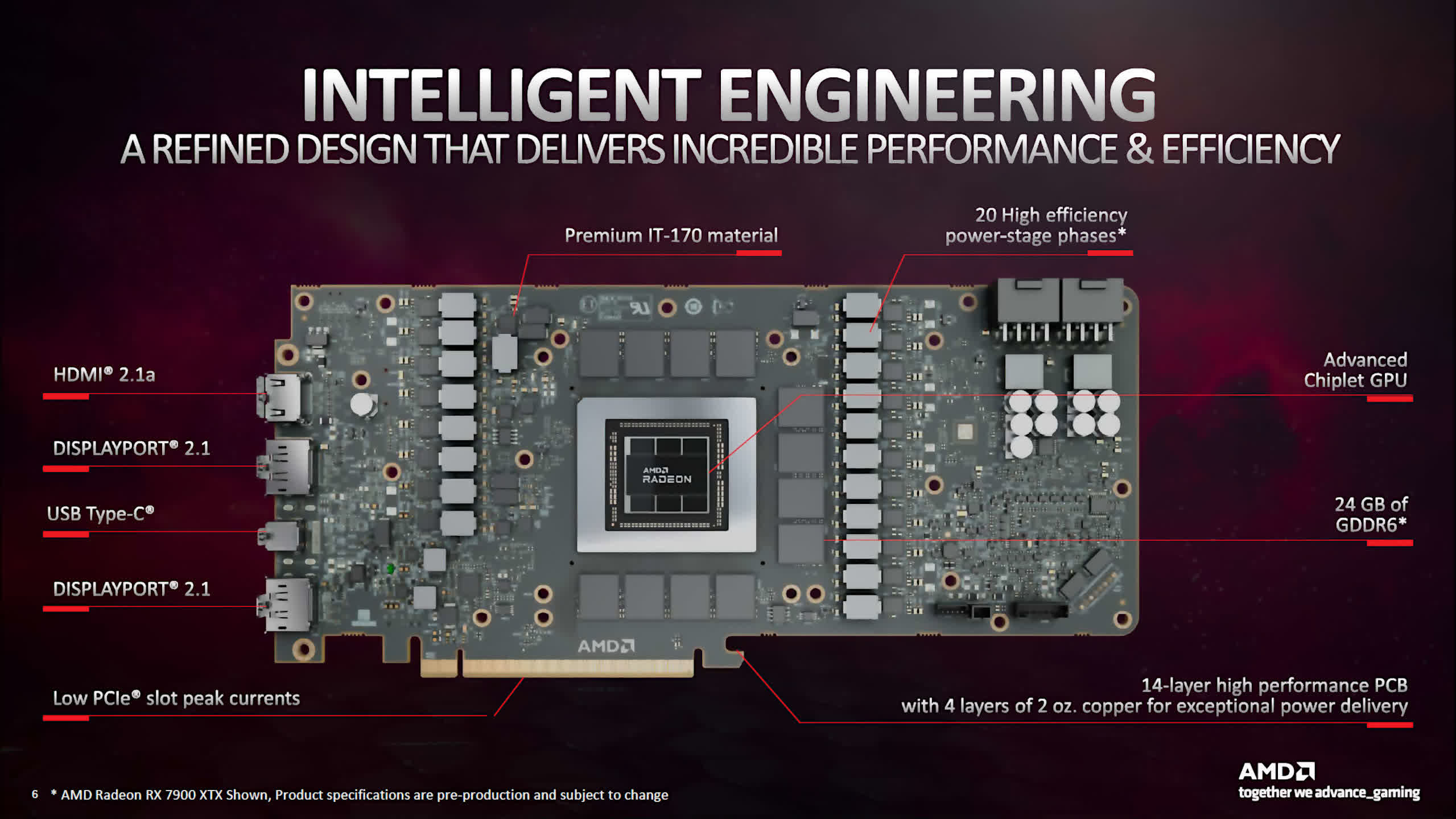
In terms of die size, the GCD is 42% smaller than the Navi 21, coming in at 300 mm2. Each MCD is just 37mm2, so the combined die area of the Navi 31 is roughly the same as its predecessor. AMD has only stated a combined transistor count, for all the chiplets, but at 58 billion, this new GPU is their ‘largest’ consumer graphics processor ever.
To connect each MCD to the GCD, AMD is using what they call High Performance Fanouts — densely packed traces, that take up a very small amount of space. The Infinity Links — AMD’s proprietary interconnect and signaling system — run at up to 9.2Gb/s and with each MCD having a link width of 384 bits, the MCD-to-GCD bandwidth comes to 883GB/s (bidirectional).
That’s equivalent to the global memory bandwidth of a high-end graphics card, for just a single MCD. With all six in the Navi 31, the combined L2-to-MCD bandwidth comes to 5.3TB/s.
The use of complex fanouts means the cost of die packaging, compared to a traditional monolithic chip, is going to be higher but the process is scalable — different SKUs can use the same GCD but varying numbers of MCDs. The smaller sizes of the individual chiplet dies should improve wafer yields, but there’s no indication as to whether AMD has incorporated any redundancy into the design of the MCDs.
If there isn’t any, it means any chiplet that has flaws in the SRAM, which prevent that part of the memory array from being used, then they will have to be binned for a lower-end model SKU or not used at all.
AMD has only announced two RDNA 3 graphics cards so far (Radeon RX 7900 XT and XTX), but in both models, the MCDs field 16MB of cache each. If the next round of Radeon cards sports a 256 bit memory bus and, say, 64MB of L3 cache, then they will need to use the ‘perfect’ 16MB dies, too.
However, since they are so small in area, a single 300mm wafer could potentially yield over 1500 MCDs. Even if 50% of those have to be scrapped, that’s still sufficient dies to furnish 125 Navi 31 packages.
It will take some time before we can tell just how cost-effective AMD’s design actually is, but the company is fully committed to using this approach now and in the future, though only for the larger GPUs. Budget RNDA 3 models, with far smaller amounts of cache, will continue to use a monolithic fabrication method as it’s more cost-effective to make them that way.
Intel’s ACM-G10 processor is 406mm2, with a total transistor count of 21.7 billion, sitting somewhere between AMD’s Navi 21 and Nvidia’s GA104, in terms of component count and die area.
This actually makes it quite a large processor, which is why Intel’s choice of market sector for the GPU seems somewhat odd. The Arc A770 graphics card, which uses a full ACM-G10 die, was pitched against the likes of Nvidia’s GeForce RTX 3060 — a graphics card that uses a chip half the size and transistor count of Intel’s.
So why is it so large? There are two probable causes: the 16MB of L2 cache and the very large number of matrix units in each XEC. The decision to have the former is logical, as it eases pressure on the global memory bandwidth, but the latter could easily be considered excessive for the sector it’s sold in. The RTX 3060 has 112 Tensor cores, whereas the A770 has 512 XMX units.
Another odd choice by Intel is the use of TSMC N6 for manufacturing the Alchemist dies, rather than their own facilities. An official statement given on the matter cited factors such as cost, fab capacity, and chip operating frequency.
This suggests that Intel’s equivalent production facilities (using the renamed Intel 7 node) wouldn’t have been able to meet the expected demand, with their Alder and Raptor Lake CPUs taking up most of the capacity.
They would have compared the relative drop in CPU output, and how that would have impacted revenue, against what they would have gained with Alchemist. In short, it was better to pay TSMC to make its new GPUs.
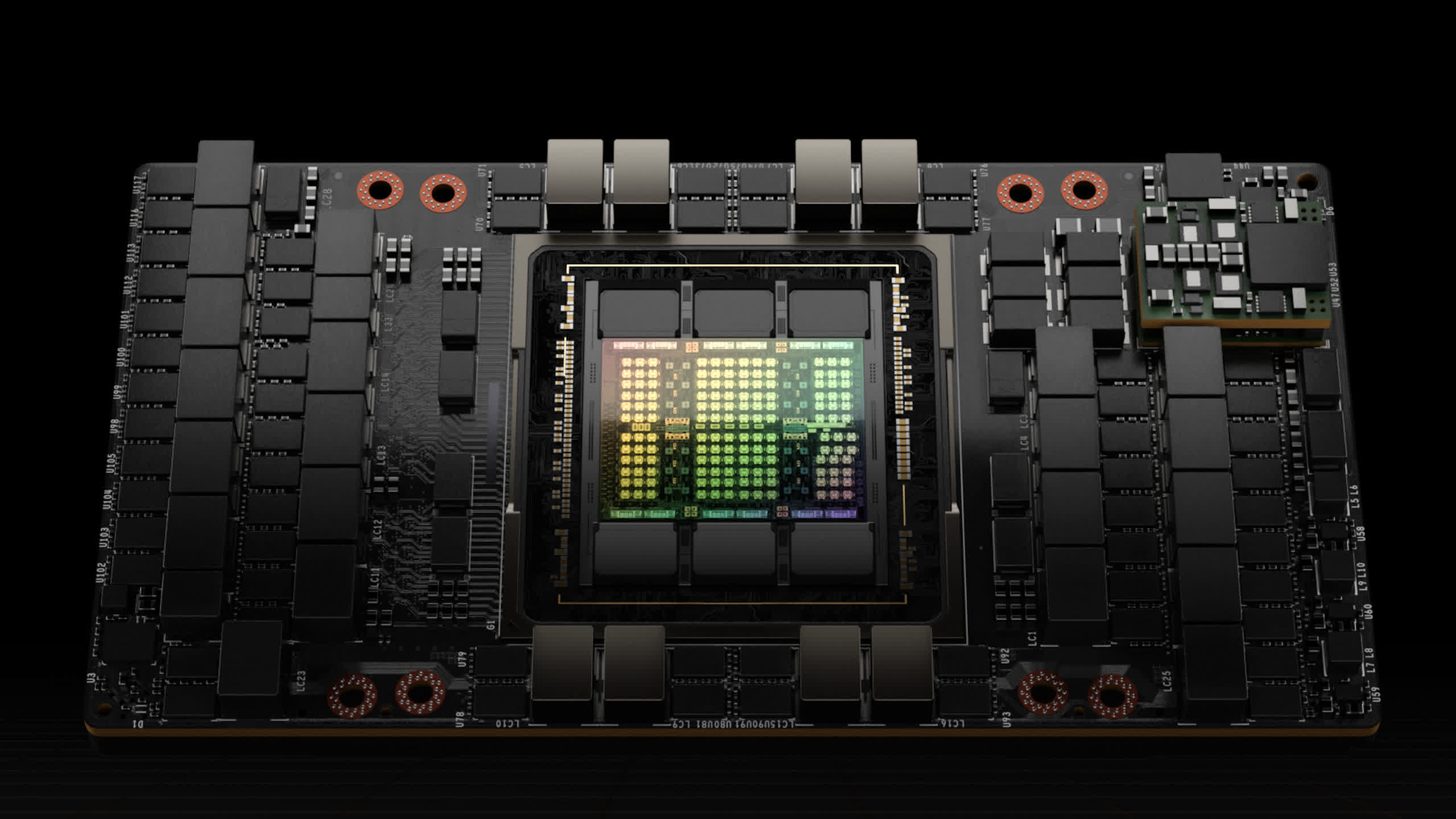
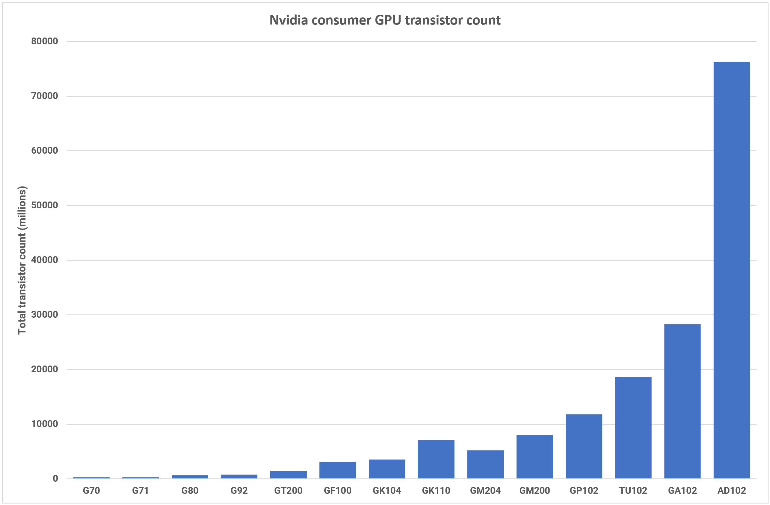
Where AMD used its multichip expertise and developed new technologies for the manufacture of large RDNA 3 GPU, Nvidia stuck with a monolithic design for the Ada lineup. The GPU company has considerable experience in creating extremely large processors, though at 608mm2 the AD102 isn’t the physically largest chip it has released (that honor goes to the GA100 at 826mm2).
However, with 76.3 billion transistors, Nvidia has pushed the component count way ahead of any consumer-grade GPU seen so far.
The GA102, used in the GeForce RTX 3080 and upwards, seems lightweight in comparison, with just 26.8 billion. This 187% increase went towards the 71% growth in SM count and the 1500% uplift in L2 cache amount.
Such a large and complex chip as this will always struggle to achieve perfect wafer yields, which is why previous top-end Nvidia GPUs have spawned a multitude of SKUs. Typically, with a new architecture launch, their professional line of graphics cards (e.g. the A-series, Tesla, etc) are announced first.
When Ampere was announced, the GA102 appeared in two consumer-grade cards at launch and went on to eventually finding a home in 14 different products. So far, Nvidia has so far chosen to use AD102 in just two: the GeForce RTX 4090 and the RTX 6000. The latter hasn’t been available for purchase since appearing in September, though.
The RTX 4090 uses dies that are towards the better end of the binning process, with 16 SMs and 24MB of L2 cache disabled, whereas the RTX 6000 has just two SMs disabled. Which leaves one to ask: where are the rest of the dies?
But with no other products using the AD102, we’re left to assume that Nvidia is stockpiling them, although for what other products isn’t clear.
The GeForce RTX 4080 uses the AD103, which at 379mm2 and 45.9 billion transistors, is nothing like its bigger brother — the much smaller die (80 SMs, 64MB L2 cache) should result in far better yields, but again there’s only the one product using it.
They also announced another RTX 4080, one using the smaller-still AD104, but back-tracked on that launch due to the weight of criticism they received. It’s expected that this GPU will now be used to launch the RTX 4070 lineup.
Nvidia clearly has plenty of GPUs built on the Ada architecture but also seems very reluctant to ship them. One reason for this could be that they’re waiting for Ampere-powered graphics cards to clear the shelves; another is the fact that it dominates the general user and workstation markets, and possibly feels that it doesn’t need to offer anything else right now.
But given the substantial improvement in raw compute capability that both the AD102 and 103 offer, it’s somewhat puzzling that there are so few Ada professional cards — the sector is always hungry for more processing power.
Superstar DJs: Display and Media Engines
When it comes to the media & display engines of GPUs, they often receive a back-of-the-stage marketing approach, compared to aspects such as DirectX 12 features or transistor count. But with the game streaming industry generating billions of dollars in revenue, we’re starting to see more effort being made to develop and promote new display features.
For RDNA 3, AMD updated a number of components, the most notable being support for DisplayPort 2.1 (as well as HDMI 2.1a). Given that VESA, the organization that oversees the DisplayPort specification, only announced the 2.1 version a few months ago, it was an unusual move for a GPU vendor to adopt the system so quickly.
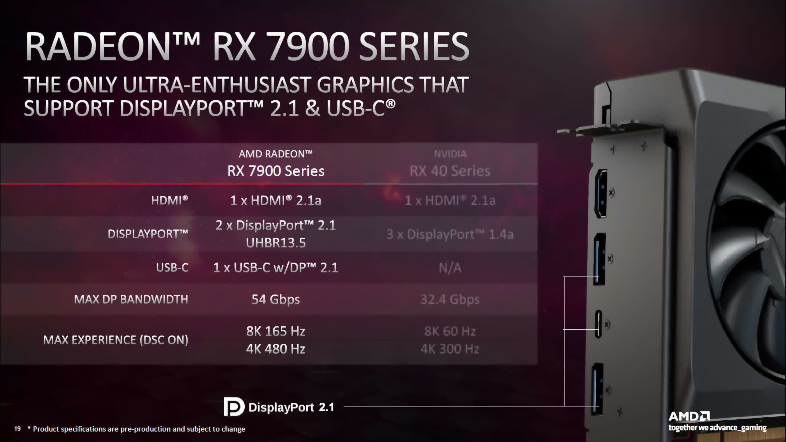
The fastest DP transmission mode the new display engine supports is UHBR13.5, giving a maximum 4-lane transmission rate of 54 Gbps. This is good enough for a resolution of 4K, at a refresh rate of 144Hz, without any compression, on standard timings.
Using DSC (Display Stream Compression), the DP2.1 connections permit up to 4K@480Hz or 8K@165Hz — a notable improvement over DP1.4a, as used in RDNA 2.
Intel’s Alchemist architecture features a display engine with DP 2.0 (UHBR10, 40 Gbps) and HDMI 2.1 outputs, although not all Arc-series graphics cards using the chip may utilize the maximum capabilities.
While the ACM-G10 isn’t targeted at high-resolution gaming, the use of the latest display connection specifications means that e-sports monitors (e.g. 1080p, 360Hz) can be used without any compression. The chip may not be able to render such high frame rates in those kinds of games, but at least the display engine can.

AMD and Intel’s support for fast transmission modes in DP and HDMI is the sort of thing you’d expect from brand-new architectures, so it’s somewhat incongruous that Nvidia chose not to do so with Ada Lovelace.
The AD102, for all its transistors (almost the same as Navi 31 and ACM-G10 added together), only has a display engine with DP1.4a and HDMI 2.1 outputs. With DSC, the former is good enough for, say, 4K@144Hz, but when the competition supports that without compression, it’s clearly a missed opportunity.
Media engines in GPUs are responsible for the encoding and decoding of video streams, and all three vendors have fulsome feature sets in their latest architectures.
In RDNA 3, AMD added full, simultaneous encode/decode for the AV1 format (it was decode only in the previous RDNA 2). There’s not a great deal of information about the new media engines, other than it can process two H.264/H.265 streams at the same time, and the maximum rate for AV1 is 8K@60Hz. AMD also briefly mentioned ‘AI Enhanced’ video decode but provided no further details.
Intel’s ACM-G10 has a similar range of capabilities, encode/decoding available for AV1, H.264, and H.265, but just as with RDNA 3, details are very scant. Some early testing of the first Alchemist chips in Arc desktop graphics cards suggests that the media engines are as least as good as those offered by AMD and Nvidia in their previous architectures.
Ada Lovelace follows suit with AV1 encoding and decoding, and Nvidia is claiming that the new system is 40% more efficient in encoding than H.264 — ostensibly, 40% better video quality is available when using the newer format.
Top-end GeForce RTX 40 series graphics cards will come with GPUs sporting two NVENC encoders, giving you the option of encoding 8K HDR at 60Hz or improved parallelization of video exporting, with each encoder working on half a frame at the same time.
With more information about the systems, a better comparison could be made, but with media engines still being seen as the poor relations to the rendering and compute engines, we’ll have to wait until every vendor has cards with their latest architectures on shelves, before we can examine matters further.
What’s Next for the GPU?
It’s been a long time since we’ve had three vendors in the desktop GPU market and it’s clear that each one has its own approach to designing graphics processors, though Intel and Nvidia take a similar mindset.
For them, Ada and Alchemist are somewhat of a jack-of-all-trades, to be used for all kinds of gaming, scientific, media, and data workloads. The heavy emphasis on matrix and tensor calculations in the ACM-G10 and a reluctance to completely redesign their GPU layout shows that Intel is leaning more towards science and data, rather than gaming, but this is understandable, given the potential growth in these sectors.
With the last three architectures, Nvidia has focused on improving upon what was already good, and reducing various bottlenecks within the overall design, such as internal bandwidth and latencies. But while Ada is a natural refinement of Ampere, a theme that Nvidia has followed for a number of years now, the AD102 stands out as being an evolutionary oddity when you look at the sheer scale of the transistor count.
The difference compared to the GA102 is nothing short of remarkable, but this colossal leap raises a number of questions. The first of which is, would the AD103 have been a better choice for Nvidia to go with, for their highest-end consumer product, instead of the AD102?
As used in the RTX 4080, AD103’s performance is a respectable improvement over the RTX 3090, and like its bigger brother, the 64MB of L2 cache helps to offset the relatively narrow 256-bit global memory bus width.
And at 379mm2, it’s smaller than the GA104 used in the GeForce RTX 3070, so would be far more profitable to fabricate than the AD102. It also houses the same number of SMs as the GA102 and that chip eventually found a home in 15 different products.
Another question worth asking is, where does Nvidia go from here in terms of architecture and fabrication? Can they achieve a similar level of scaling, while still sticking to a monolithic die?
AMD’s choices with RDNA 3 highlight a potential route for the competition to follow. By shifting the parts of the die that scale the worst (in new process nodes) into separate chiplets, AMD has been able to successfully continue the large fab & design leap made between RDNA and RDNA 2.
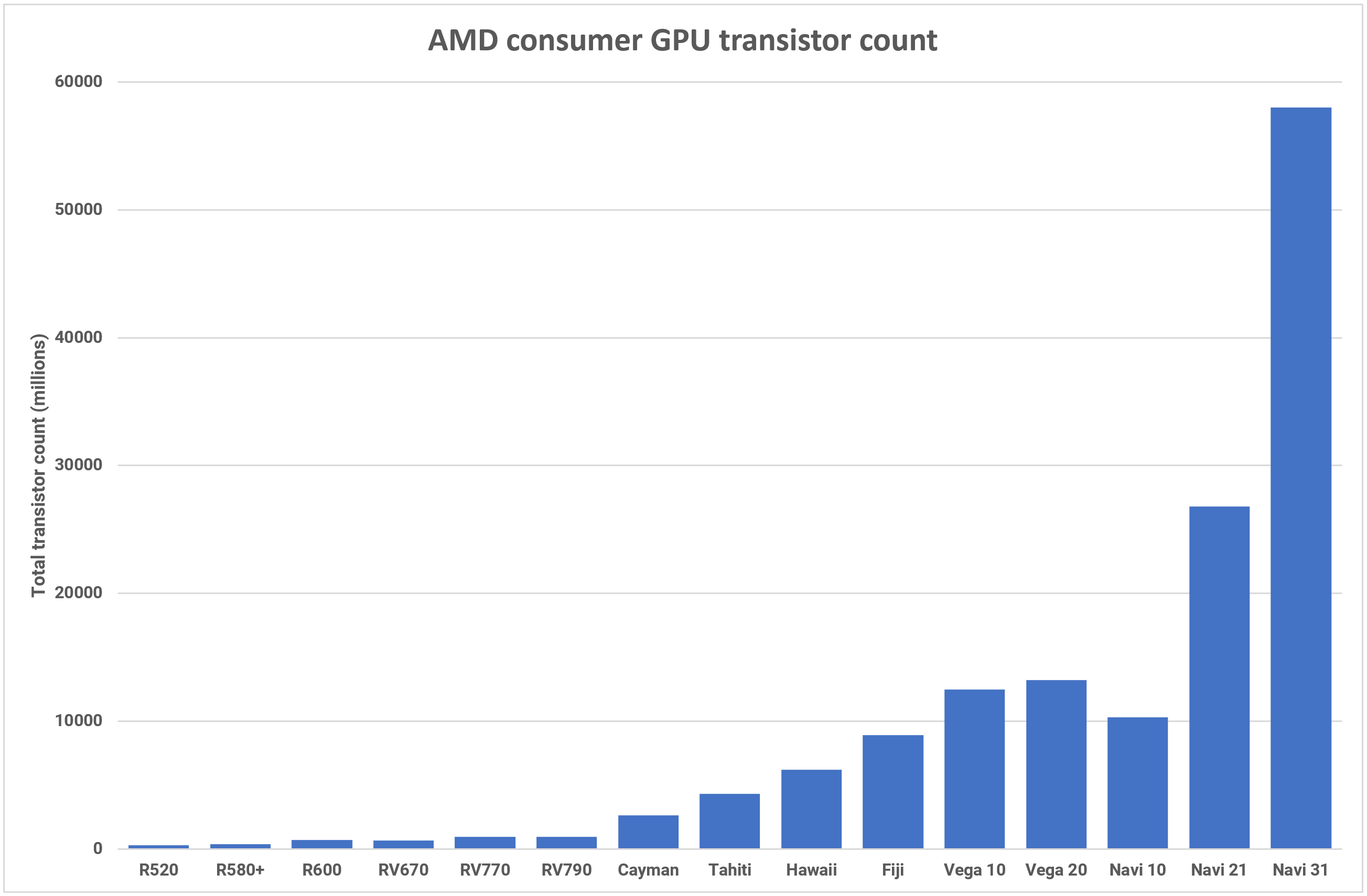
While it’s not as large as the AD102, the Navi 31 is still 58 billion transistors worth of silicon — more than double that in Navi 21, and over 5 times that in the original RDNA GPU, the Navi 10 (although that wasn’t aimed to be a halo product).
But AMD and Nvidia’s achievements were not done in isolation. Such large increases in GPU transistor counts are only possible because of the fierce competition between TSMC and Samsung for being the premier manufacturer of semiconductor devices.
Both are working towards improving the transistor density of logic circuits, while continuing to reduce power consumption, with Samsung commencing volume production of its 3nm process earlier this year. TSMC has been doing likewise and has a clear roadmap for current node refinements and their next major process.
Whether Nvidia copies a leaf from AMD’s design book and goes ahead with a chiplet layout in Ada’s successor is unclear, but the next 14 to 16 months will probably be decisive. If RDNA 3 proves to be a financial success, be it in terms of revenue or total units shipped, then there’s a distinct possibility that Nvidia follows suit.
However, the first chip to use the Ampere architecture was the GA100 — a data center GPU, 829mm2 in size and with 54.2 billion transistors. It was fabricated by TSMC, using their N7 node (the same as RDNA and most of the RDNA 2 lineup). The use of N4, to make the AD102, allowed Nvidia to design a GPU with almost double the transistor density of its predecessor.
GPUs continue to be one of the most remarkable engineering feats seen in a desktop PC
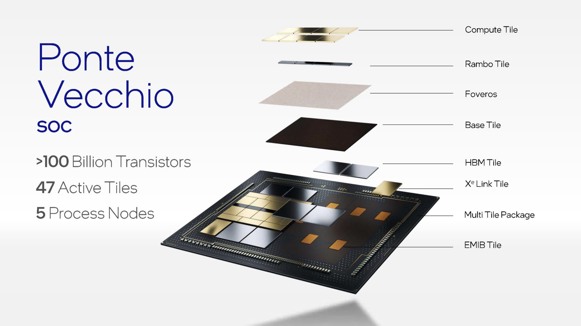
So would this be achievable using N2 for the next architecture? Possibly, but the massive growth in cache (which scales very poorly) suggests that even if TSMC achieves some remarkable figures with their future nodes, it will be increasingly harder to keep GPU sizes under control. Intel already is using chiplets, but only with its enormous Ponte Vecchio data center GPU. Composed of 47 various tiles, some fabrication by TSMC and others by Intel themselves, its parameters are suitably excessive.
For example, with more than 100 billion transistors for the full, dual-GPU configuration, it makes AMD’s Navi 31 look svelte. It is, of course, not for any kind of desktop PC nor is it strictly speaking ‘just’ a GPU — this is a data center processor, with a firm emphasis on matrix and tensor workloads.
With its Xe-HPG architecture targeted for at least two more revisions (Battlemage and Celestial) before moving on to ‘Xe Next’, we may well see the use of tiling in an Intel consumer graphics card.
For now, though, we’ll have Ada and Alchemist, using traditional monolithic dies, for at least a year or two, while AMD uses a mixture of chiplet systems for the upper-mid and top-end cards, and single dies for their budget SKUs.
By the end of the decade, though, we may see almost all kinds of graphics processors, built from a selection of different tiles/chiplets, all made using various process nodes. GPUs continue to be one of the most remarkable engineering feats seen in a desktop PC — transistor counts show no sign of tailing off in growth and the computational abilities of an average graphics card today could only be dreamed about 10 years ago.
Bring on the next three-way architecture battle!